

Voir les spécifications pour les détails du produit.
Encyclopedia Entry: 74AUP2G08GM,125
Product Overview
Category
The 74AUP2G08GM,125 belongs to the category of integrated circuits (ICs).
Use
This product is commonly used in electronic devices for signal switching and amplification purposes.
Characteristics
- Low power consumption
- High-speed operation
- Wide operating voltage range
- Small package size
Package
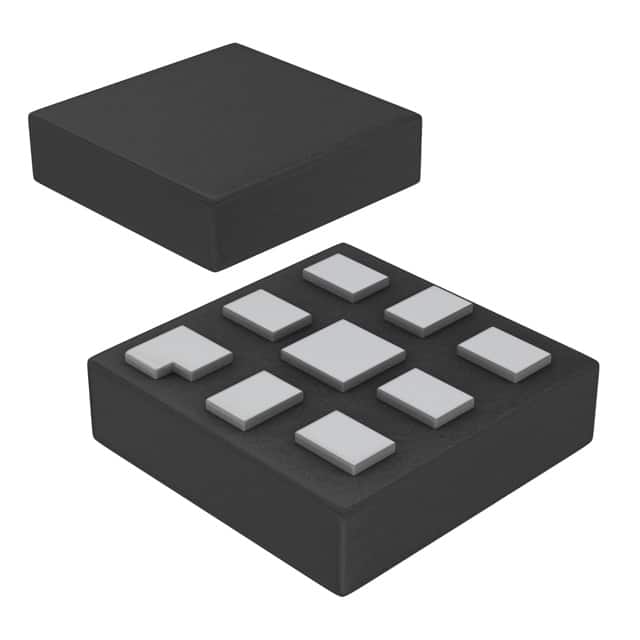
The 74AUP2G08GM,125 is available in a small package, typically a surface-mount technology (SMT) package.
Essence
The essence of this product lies in its ability to provide efficient signal switching and amplification while consuming minimal power.
Packaging/Quantity
The 74AUP2G08GM,125 is usually packaged in reels or tubes, with a quantity of around 3000 units per reel/tube.
Specifications
- Supply Voltage Range: 1.65V to 5.5V
- Input Voltage Range: 0V to VCC
- Output Voltage Range: 0V to VCC
- Operating Temperature Range: -40°C to +85°C
- Maximum Propagation Delay: 3.5ns
Detailed Pin Configuration
The 74AUP2G08GM,125 has a total of 6 pins, which are as follows:
- Pin 1: Input A
- Pin 2: Input B
- Pin 3: Ground (GND)
- Pin 4: Output Y
- Pin 5: Power Supply (VCC)
- Pin 6: No Connection (NC)
Functional Features
- Dual 2-input AND gate functionality
- High-speed operation allows for quick signal processing
- Low power consumption makes it suitable for battery-powered devices
- Wide operating voltage range enables compatibility with various systems
Advantages and Disadvantages
Advantages
- Low power consumption helps prolong battery life in portable devices.
- High-speed operation ensures efficient signal processing.
- Wide operating voltage range provides flexibility in system integration.
Disadvantages
- Limited number of inputs (2-input AND gate) may not be suitable for complex logic operations.
- Small package size may require careful handling during assembly.
Working Principles
The 74AUP2G08GM,125 operates based on the principles of digital logic gates. It utilizes two input signals (A and B) and produces an output signal (Y) based on the logical AND operation between the inputs. The internal circuitry of the IC allows for fast and accurate signal switching.
Detailed Application Field Plans
The 74AUP2G08GM,125 finds applications in various electronic devices and systems, including but not limited to: - Mobile phones - Tablets - Digital cameras - Portable gaming consoles - Automotive electronics - Industrial control systems
Detailed and Complete Alternative Models
Some alternative models that offer similar functionality to the 74AUP2G08GM,125 include: - 74HC08: A standard CMOS quad 2-input AND gate - SN74LS08: A TTL quad 2-input AND gate - CD4081: A CMOS quad 2-input AND gate
These alternative models can be considered depending on specific requirements and compatibility with existing systems.
In conclusion, the 74AUP2G08GM,125 is a versatile integrated circuit that provides efficient signal switching and amplification capabilities. Its low power consumption, high-speed operation, and wide operating voltage range make it suitable for various electronic applications. However, its limited number of inputs and small package size should be taken into consideration when selecting this product for specific projects.
Énumérez 10 questions et réponses courantes liées à l'application de 74AUP2G08GM,125 dans les solutions techniques
Sure! Here are 10 common questions and answers related to the application of 74AUP2G08GM,125 in technical solutions:
Q: What is the 74AUP2G08GM,125? A: The 74AUP2G08GM,125 is a dual 2-input AND gate integrated circuit (IC) that can be used in various electronic applications.
Q: What is the operating voltage range for the 74AUP2G08GM,125? A: The operating voltage range for this IC is typically between 0.8V and 3.6V.
Q: What is the maximum output current of the 74AUP2G08GM,125? A: The maximum output current is around 32mA.
Q: Can the 74AUP2G08GM,125 be used in battery-powered devices? A: Yes, it can be used in battery-powered devices due to its low power consumption and wide operating voltage range.
Q: What is the typical propagation delay of the 74AUP2G08GM,125? A: The typical propagation delay is around 2.5ns.
Q: Is the 74AUP2G08GM,125 compatible with other logic families? A: Yes, it is compatible with both CMOS and TTL logic families.
Q: Can the 74AUP2G08GM,125 drive capacitive loads? A: Yes, it can drive small capacitive loads without requiring additional buffering.
Q: What is the package type for the 74AUP2G08GM,125? A: It is available in a small SOT353 package.
Q: Can the 74AUP2G08GM,125 be used in high-speed applications? A: Yes, it can be used in high-speed applications due to its low propagation delay and fast switching characteristics.
Q: What are some common applications for the 74AUP2G08GM,125? A: Some common applications include signal conditioning, level shifting, digital logic gates, and general-purpose digital circuitry.
Please note that the answers provided here are general and may vary depending on specific datasheet specifications and application requirements.