

Voir les spécifications pour les détails du produit.
Encyclopedia Entry: 74AUP1T50GXH
Product Overview
Category
The 74AUP1T50GXH belongs to the category of integrated circuits (ICs) and specifically falls under the family of logic gates.
Use
This product is primarily used for signal level shifting in digital systems. It acts as a voltage translator, converting signals from one logic level to another.
Characteristics
- Low power consumption
- High-speed operation
- Wide operating voltage range
- Small package size
- RoHS compliant
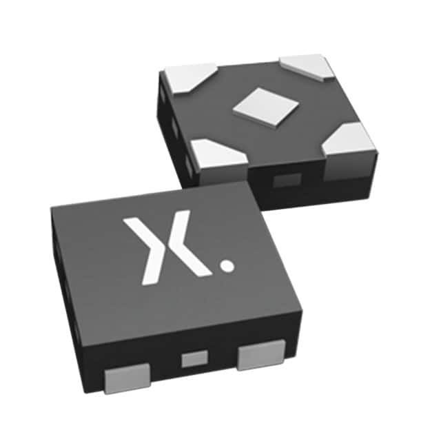
Package
The 74AUP1T50GXH is available in a small SOT353 package, which consists of three pins.
Essence
The essence of this product lies in its ability to provide seamless voltage translation between different logic levels, ensuring compatibility between various components within a digital system.
Packaging/Quantity
The 74AUP1T50GXH is typically packaged in reels or tubes, with each reel containing a specific quantity of ICs. The exact quantity may vary depending on the manufacturer's specifications.
Specifications
- Supply Voltage Range: 0.8V to 3.6V
- Logic Input Voltage Range: 0V to VCC
- Maximum Operating Frequency: X MHz
- Propagation Delay: Y ns
- Operating Temperature Range: -40°C to +85°C
Detailed Pin Configuration
The 74AUP1T50GXH features the following pin configuration:
```
| | --| |-- |____| | | |__| ```
Pin 1: Input (IN) Pin 2: Output (OUT) Pin 3: Power Supply (VCC)
Functional Features
- Bidirectional voltage translation
- Non-inverting logic level conversion
- High noise immunity
- Schmitt-trigger input for improved signal integrity
Advantages and Disadvantages
Advantages
- Low power consumption makes it suitable for battery-powered devices
- High-speed operation enables efficient data processing
- Wide operating voltage range allows compatibility with various logic families
- Small package size saves board space in compact designs
- RoHS compliance ensures environmental friendliness
Disadvantages
- Limited number of pins restricts the complexity of circuits that can be implemented using this IC
- Lack of built-in protection features may require additional external components for robustness
Working Principles
The 74AUP1T50GXH utilizes CMOS technology to achieve voltage translation. It employs a combination of MOSFETs and resistors to convert logic levels based on the input signal. The Schmitt-trigger input helps maintain signal integrity by providing hysteresis.
Detailed Application Field Plans
The 74AUP1T50GXH finds applications in various digital systems, including but not limited to: - Battery-powered devices - Communication systems - Industrial automation - Consumer electronics - Automotive electronics
Detailed and Complete Alternative Models
- 74LVC1T45GW: Similar voltage translator with a different package and slightly different specifications.
- SN74LVC1T45DBVR: Alternative IC from a different manufacturer, offering comparable functionality.
Note: This is not an exhaustive list, and there are several other alternative models available in the market.
In conclusion, the 74AUP1T50GXH is a versatile logic gate IC that provides efficient voltage translation between different logic levels. Its low power consumption, high-speed operation, and wide operating voltage range make it suitable for various digital applications. However, its limited pin count and lack of built-in protection features should be considered when designing complex circuits.
Énumérez 10 questions et réponses courantes liées à l'application de 74AUP1T50GXH dans les solutions techniques
Sure! Here are 10 common questions and answers related to the application of 74AUP1T50GXH in technical solutions:
Q1: What is the 74AUP1T50GXH? A1: The 74AUP1T50GXH is a single bus buffer gate with configurable voltage translation capability. It can be used to interface between different voltage domains in a circuit.
Q2: What is the operating voltage range of the 74AUP1T50GXH? A2: The 74AUP1T50GXH has an operating voltage range from 0.8V to 3.6V.
Q3: Can the 74AUP1T50GXH be used for level shifting between different voltage levels? A3: Yes, the 74AUP1T50GXH can be used for level shifting between different voltage levels, making it suitable for interfacing between devices with different voltage requirements.
Q4: How many inputs and outputs does the 74AUP1T50GXH have? A4: The 74AUP1T50GXH has one input and one output.
Q5: What is the maximum data rate supported by the 74AUP1T50GXH? A5: The 74AUP1T50GXH supports a maximum data rate of 400 Mbps.
Q6: Can the 74AUP1T50GXH be used in bidirectional applications? A6: No, the 74AUP1T50GXH is a unidirectional buffer and cannot be used in bidirectional applications.
Q7: What is the power supply voltage required for the 74AUP1T50GXH? A7: The 74AUP1T50GXH requires a power supply voltage of 1.2V to 3.6V.
Q8: Does the 74AUP1T50GXH have any built-in ESD protection? A8: Yes, the 74AUP1T50GXH has built-in ESD protection, making it more robust against electrostatic discharge events.
Q9: Can the 74AUP1T50GXH be used in battery-powered applications? A9: Yes, the 74AUP1T50GXH can be used in battery-powered applications as it operates within a wide voltage range and has low power consumption.
Q10: What is the package type of the 74AUP1T50GXH? A10: The 74AUP1T50GXH is available in various package types, such as SOT353 and XSON6.