

Voir les spécifications pour les détails du produit.
Encyclopedia Entry: 74AUP1G885GN,115
Product Overview
Category
The 74AUP1G885GN,115 belongs to the category of integrated circuits (ICs).
Use
This product is commonly used in electronic devices for signal switching and amplification.
Characteristics
- Low power consumption
- High-speed operation
- Small form factor
- Wide operating voltage range
Package
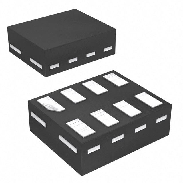
The 74AUP1G885GN,115 is available in a compact SOT353 package.
Essence
The essence of this product lies in its ability to provide efficient signal switching and amplification in various electronic applications.
Packaging/Quantity
The 74AUP1G885GN,115 is typically packaged in reels containing a quantity of 3000 units.
Specifications
- Supply Voltage Range: 0.8V to 3.6V
- Operating Temperature Range: -40°C to +85°C
- Input Capacitance: 2.5pF
- Output Capacitance: 2.5pF
- Propagation Delay Time: 2.5ns
- Maximum Power Dissipation: 150mW
Detailed Pin Configuration
The 74AUP1G885GN,115 has the following pin configuration:
```
| | --| IN / OUT |-- Pin 1 --| GND |-- Pin 2 --| VCC |-- Pin 3 |___________| ```
Functional Features
- Single-channel signal switching
- High-speed operation for quick response times
- Low power consumption for energy efficiency
- Wide operating voltage range for compatibility with different systems
Advantages and Disadvantages
Advantages
- Compact size allows for space-saving designs
- Low power consumption prolongs battery life
- High-speed operation enables efficient signal processing
Disadvantages
- Limited number of channels for simultaneous switching
- May require additional components for complex circuit designs
Working Principles
The 74AUP1G885GN,115 operates based on the principles of semiconductor technology. It utilizes MOSFET transistors to control the flow of signals, enabling efficient switching and amplification.
Detailed Application Field Plans
The 74AUP1G885GN,115 finds applications in various electronic devices, including but not limited to: - Mobile phones - Tablets - Portable media players - Wearable devices - IoT (Internet of Things) devices
Detailed and Complete Alternative Models
Some alternative models that can be considered as alternatives to the 74AUP1G885GN,115 include: - 74LVC1G125GW,125 - 74HC1G14GW,125 - 74LV1T34GW,125 - 74LVC1G07GW,125
These alternative models offer similar functionality and characteristics, providing flexibility in design choices.
In conclusion, the 74AUP1G885GN,115 is a compact and efficient integrated circuit used for signal switching and amplification in various electronic devices. Its low power consumption, high-speed operation, and wide operating voltage range make it suitable for a range of applications. While it has some limitations in terms of channel count, it offers advantages such as space-saving design and energy efficiency.
Énumérez 10 questions et réponses courantes liées à l'application de 74AUP1G885GN,115 dans les solutions techniques
Sure! Here are 10 common questions and answers related to the application of 74AUP1G885GN,115 in technical solutions:
Q1: What is the 74AUP1G885GN,115? A1: The 74AUP1G885GN,115 is a single buffer/driver IC (integrated circuit) that can be used in various technical solutions.
Q2: What is the purpose of the 74AUP1G885GN,115? A2: The purpose of this IC is to provide buffering or driving capabilities for signals in electronic circuits.
Q3: What voltage levels does the 74AUP1G885GN,115 support? A3: The 74AUP1G885GN,115 supports voltage levels ranging from 0.8V to 3.6V.
Q4: What is the maximum output current of the 74AUP1G885GN,115? A4: The maximum output current of this IC is typically around 32mA.
Q5: Can the 74AUP1G885GN,115 be used in battery-powered applications? A5: Yes, this IC can be used in battery-powered applications as it operates at low power supply voltages.
Q6: Is the 74AUP1G885GN,115 compatible with other logic families? A6: Yes, this IC is compatible with various logic families such as CMOS, TTL, and LVCMOS.
Q7: What is the operating temperature range of the 74AUP1G885GN,115? A7: The operating temperature range of this IC is typically between -40°C to +125°C.
Q8: Can the 74AUP1G885GN,115 be used in high-speed applications? A8: Yes, this IC can be used in high-speed applications as it has a fast propagation delay.
Q9: Does the 74AUP1G885GN,115 have any built-in protection features? A9: Yes, this IC has built-in ESD (electrostatic discharge) protection to safeguard against static electricity.
Q10: What is the package type of the 74AUP1G885GN,115? A10: The 74AUP1G885GN,115 is available in a small SOT353 package.
Please note that the answers provided here are general and may vary depending on the specific datasheet and application requirements.