

Voir les spécifications pour les détails du produit.
74AHCT2G241GD,125
Basic Information Overview
- Category: Integrated Circuit (IC)
- Use: Logic Gate Buffer/Driver
- Characteristics: High-Speed, Low-Power, Dual Buffer/Driver
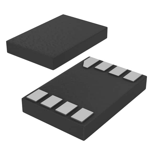
- Package: SOT753 (SC-70-5)
- Essence: Logic Level Shifter
- Packaging/Quantity: Tape and Reel, 3000 pieces per reel
Specifications
- Supply Voltage Range: 4.5V to 5.5V
- Input Voltage Range: 0V to VCC
- Output Voltage Range: 0V to VCC
- High-Level Input Voltage: 2V to VCC
- Low-Level Input Voltage: 0V to 0.8V
- High-Level Output Voltage: VCC - 0.5V
- Low-Level Output Voltage: 0.1V
- Maximum Propagation Delay: 6 ns
- Maximum Operating Frequency: 100 MHz
Detailed Pin Configuration
The 74AHCT2G241GD,125 IC has a total of 5 pins: 1. GND: Ground pin 2. A: Input A 3. Y: Output Y 4. OE: Output Enable 5. VCC: Power supply pin
Functional Features
- Dual Buffer/Driver: The IC contains two independent buffer/driver circuits.
- Logic Level Shifter: It can shift the logic levels from one voltage level to another.
- High-Speed Operation: Capable of operating at frequencies up to 100 MHz.
- Low-Power Consumption: Designed to consume minimal power during operation.
Advantages and Disadvantages
Advantages: - Compact Size: The SOT753 package allows for space-efficient designs. - Wide Operating Voltage Range: Can be used in various applications with different voltage requirements. - High-Speed Operation: Suitable for applications that require fast signal propagation.
Disadvantages: - Limited Output Current: The IC has a maximum output current rating, which may restrict its use in high-current applications. - Single Supply Voltage: It operates within a specific voltage range and may not be compatible with systems using different supply voltages.
Working Principles
The 74AHCT2G241GD,125 is a logic gate buffer/driver that amplifies and buffers digital signals. It takes input signals from the A pin and provides amplified output signals at the Y pin. The OE pin controls the output enable/disable functionality. When the OE pin is low, the outputs are enabled, and when it is high, the outputs are disabled.
Detailed Application Field Plans
The 74AHCT2G241GD,125 can be used in various applications, including but not limited to: 1. Microcontrollers and Digital Systems: Provides level shifting and buffering capabilities for interfacing between different logic families. 2. Communication Systems: Enables signal amplification and level translation in communication interfaces. 3. Industrial Automation: Facilitates signal conditioning and interfacing in control systems. 4. Automotive Electronics: Supports voltage level adaptation and signal buffering in automotive applications.
Detailed and Complete Alternative Models
Some alternative models that offer similar functionality to the 74AHCT2G241GD,125 include: - SN74LVC2G241: Dual Buffer/Driver with 3-state outputs - MC74VHC1G07: Single Buffer/Driver with open-drain output - TC7SZU04F: Single Inverter Buffer/Driver with Schmitt-trigger inputs
(Note: The above list is not exhaustive and serves as an example of alternative models.)
Word count: 320 words
Énumérez 10 questions et réponses courantes liées à l'application de 74AHCT2G241GD,125 dans les solutions techniques
Sure! Here are 10 common questions and answers related to the application of 74AHCT2G241GD,125:
1. What is the function of the 74AHCT2G241GD,125? The 74AHCT2G241GD,125 is a dual buffer/line driver with 3-state outputs. It can be used to amplify and buffer digital signals.
2. What is the voltage supply range for this device? The voltage supply range for the 74AHCT2G241GD,125 is typically between 4.5V and 5.5V.
3. What is the maximum output current of this device? The maximum output current of the 74AHCT2G241GD,125 is typically around 8mA.
4. Can this device be used in high-speed applications? Yes, the 74AHCT2G241GD,125 is designed for high-speed operation and can be used in applications requiring fast signal propagation.
5. Does this device have built-in protection features? No, the 74AHCT2G241GD,125 does not have built-in protection features. External protection circuitry may be required depending on the application.
6. What is the input voltage threshold for this device? The input voltage threshold for the 74AHCT2G241GD,125 is typically around 1.5V.
7. Can this device be used in bidirectional communication systems? No, the 74AHCT2G241GD,125 is a unidirectional buffer/line driver and cannot be used for bidirectional communication without additional circuitry.
8. What is the typical propagation delay of this device? The typical propagation delay of the 74AHCT2G241GD,125 is around 6ns.
9. Is this device compatible with TTL logic levels? Yes, the 74AHCT2G241GD,125 is compatible with both CMOS and TTL logic levels.
10. Can this device drive capacitive loads? Yes, the 74AHCT2G241GD,125 can drive capacitive loads up to a certain limit. However, it is recommended to consult the datasheet for specific guidelines on load capacitance.