

Voir les spécifications pour les détails du produit.
Encyclopedia Entry: 74AHCT1G79GV,125
Product Overview
Category
The 74AHCT1G79GV,125 belongs to the category of integrated circuits (ICs).
Use
This product is commonly used in electronic devices for signal processing and amplification.
Characteristics
- Low power consumption
- High-speed operation
- Wide operating voltage range
- Small package size
Package
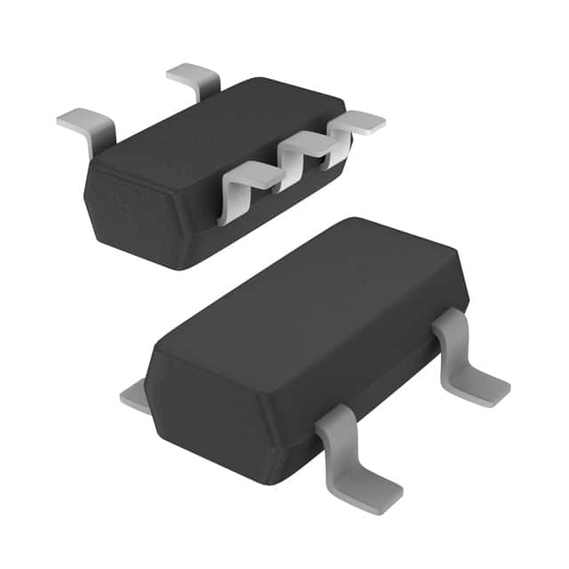
The 74AHCT1G79GV,125 is available in a small SOT-23 package.
Essence
This integrated circuit serves as a dual positive-edge triggered D-type flip-flop.
Packaging/Quantity
The 74AHCT1G79GV,125 is typically packaged in reels containing 3000 units.
Specifications
- Supply Voltage Range: 2.0V to 5.5V
- Input Voltage Range: -0.5V to VCC + 0.5V
- Operating Temperature Range: -40°C to +85°C
- Output Current: ±8mA
- Propagation Delay: 6ns (typical)
Detailed Pin Configuration
The 74AHCT1G79GV,125 has the following pin configuration:
____
CLR --|    |
D   --|    |
CLK --|    |
Q   --|    |
     --|____|
Functional Features
- Dual positive-edge triggered D-type flip-flop
- Asynchronous clear input (CLR)
- Synchronous data input (D)
- Synchronous clock input (CLK)
- Complementary outputs (Q and Q̅)
Advantages and Disadvantages
Advantages
- Low power consumption makes it suitable for battery-powered devices.
- High-speed operation enables efficient signal processing.
- Wide operating voltage range allows compatibility with various systems.
- Small package size saves board space in compact designs.
Disadvantages
- Limited number of flip-flops per package.
- Not suitable for applications requiring a large number of sequential logic elements.
Working Principles
The 74AHCT1G79GV,125 operates as a positive-edge triggered D-type flip-flop. The data input (D) is latched and transferred to the output (Q) on the rising edge of the clock input (CLK). The asynchronous clear input (CLR) resets the flip-flop to its initial state when activated.
Detailed Application Field Plans
The 74AHCT1G79GV,125 can be used in various applications, including: 1. Digital communication systems 2. Microcontrollers and microprocessors 3. Data storage devices 4. Industrial automation systems 5. Consumer electronics
Detailed and Complete Alternative Models
Some alternative models that serve similar functions to the 74AHCT1G79GV,125 include: - SN74LVC1G79DBVR - MC74VHC1G79DTT1G - TC7SZ79FU(T5L,F)
These alternatives offer comparable features and can be used as substitutes depending on specific requirements.
Word count: 345 words
Énumérez 10 questions et réponses courantes liées à l'application de 74AHCT1G79GV,125 dans les solutions techniques
Sure! Here are 10 common questions and answers related to the application of 74AHCT1G79GV,125 in technical solutions:
Q1: What is the function of the 74AHCT1G79GV,125? A1: The 74AHCT1G79GV,125 is a single positive-edge triggered D-type flip-flop with reset. It can store a single bit of data and has a reset input.
Q2: What is the voltage supply range for this IC? A2: The 74AHCT1G79GV,125 operates within a voltage supply range of 4.5V to 5.5V.
Q3: How many inputs and outputs does it have? A3: This IC has one data input (D), one clock input (CLK), one reset input (R), and one output (Q).
Q4: What is the maximum clock frequency it can handle? A4: The 74AHCT1G79GV,125 can handle clock frequencies up to 125 MHz.
Q5: Can I use this IC in battery-powered applications? A5: Yes, the 74AHCT1G79GV,125 is suitable for battery-powered applications as it operates within a low voltage range.
Q6: How does the reset input work? A6: When the reset input (R) is set to a low logic level, it resets the flip-flop and sets the output (Q) to a low logic level.
Q7: Can I cascade multiple 74AHCT1G79GV,125 flip-flops together? A7: Yes, you can cascade multiple flip-flops by connecting the output (Q) of one flip-flop to the data input (D) of the next flip-flop.
Q8: What is the typical propagation delay of this IC? A8: The typical propagation delay of the 74AHCT1G79GV,125 is around 5 ns.
Q9: Can I use this IC in high-speed applications? A9: Yes, the 74AHCT1G79GV,125 is suitable for high-speed applications due to its low propagation delay and high clock frequency capability.
Q10: Are there any recommended decoupling capacitors for this IC? A10: It is generally recommended to use decoupling capacitors near the power supply pins (VCC and GND) to minimize noise and ensure stable operation. The specific values depend on the application and should be determined based on the datasheet guidelines.
Please note that these answers are general and may vary depending on the specific requirements and conditions of your technical solution. Always refer to the datasheet and consult with an expert when designing your circuit.