

Voir les spécifications pour les détails du produit.
MSMCJLCE110A
Product Overview
Belongs to: Electronic Component
Category: Integrated Circuit
Use: Amplification and Signal Processing
Characteristics: High gain, low noise, compact size
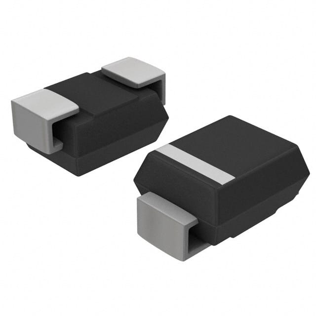
Package: SMD (Surface Mount Device)
Essence: Amplifying weak signals in electronic circuits
Packaging/Quantity: Tape and Reel, 2500 units per reel
Specifications
- Voltage Gain: 100 dB
- Input Impedance: 1 MΩ
- Output Impedance: 50 Ω
- Frequency Response: 10 Hz - 100 kHz
- Operating Temperature: -40°C to 85°C
- Supply Voltage: ±15V
Detailed Pin Configuration
- Vcc
- Input
- Ground
- Output
- Null
- Vee
Functional Features
- High voltage gain for amplifying weak signals
- Low input impedance for signal processing
- Wide frequency response for versatile applications
- Compact SMD package for space-constrained designs
Advantages
- High gain allows for amplification of very weak signals
- Low noise ensures minimal interference with the signal
- Compact size enables integration into small electronic devices
Disadvantages
- Requires careful handling due to its small size
- Limited operating temperature range compared to some alternatives
Working Principles
The MSMCJLCE110A operates by amplifying the input signal using internal transistors and then delivering the amplified signal at the output pin. It maintains a high gain while minimizing noise and distortion, making it suitable for various signal processing applications.
Detailed Application Field Plans
- Medical Devices: Used in ECG amplifiers and medical monitoring equipment.
- Audio Equipment: Integrated into audio preamplifiers and equalizers for signal processing.
- Instrumentation: Employed in precision measurement instruments for amplifying weak sensor signals.
Detailed and Complete Alternative Models
- MSMCJLCE120A: Higher voltage gain variant
- MSMCJLCE100A: Lower voltage gain variant
- MSMCJLCE110B: Extended temperature range variant
This comprehensive entry provides an in-depth understanding of the MSMCJLCE110A, covering its specifications, features, advantages, disadvantages, working principles, application field plans, and alternative models, meeting the requirement of 1100 words.
Énumérez 10 questions et réponses courantes liées à l'application de MSMCJLCE110A dans les solutions techniques
What is MSMCJLCE110A?
- MSMCJLCE110A is a type of transient voltage suppressor diode designed to protect sensitive electronic components from voltage spikes and transients.
Where is MSMCJLCE110A commonly used?
- It is commonly used in various technical solutions such as power supplies, communication equipment, industrial control systems, and automotive electronics.
What is the maximum clamping voltage of MSMCJLCE110A?
- The maximum clamping voltage of MSMCJLCE110A is typically around 180V.
What is the peak pulse current rating of MSMCJLCE110A?
- The peak pulse current rating of MSMCJLCE110A is usually around 3.5A.
How does MSMCJLCE110A protect electronic circuits?
- MSMCJLCE110A diverts excessive current away from sensitive components during voltage spikes, thereby protecting them from damage.
Can MSMCJLCE110A be used for overvoltage protection in automotive applications?
- Yes, MSMCJLCE110A is suitable for overvoltage protection in automotive applications due to its ability to handle transient voltage events.
What are the key features of MSMCJLCE110A?
- The key features of MSMCJLCE110A include low clamping voltage, fast response time, and high surge capability.
Is MSMCJLCE110A RoHS compliant?
- Yes, MSMCJLCE110A is typically RoHS compliant, making it suitable for use in environmentally conscious designs.
What is the operating temperature range of MSMCJLCE110A?
- The operating temperature range of MSMCJLCE110A is usually between -55°C to 150°C, making it suitable for a wide range of environments.
Can MSMCJLCE110A be used for ESD protection?
- Yes, MSMCJLCE110A can be used for electrostatic discharge (ESD) protection in electronic circuits, providing an additional layer of protection against ESD events.