

Voir les spécifications pour les détails du produit.
A40MX02-1PQG100M
Product Overview
Category
A40MX02-1PQG100M belongs to the category of programmable logic devices (PLDs).
Use
This product is commonly used in digital circuit design and implementation. It provides a flexible and customizable solution for various applications.
Characteristics
- Programmable: The A40MX02-1PQG100M can be programmed to perform specific functions based on the user's requirements.
- High Integration: It offers a high level of integration, allowing multiple functions to be implemented within a single device.
- Versatile: This PLD supports a wide range of applications due to its programmability.
- Low Power Consumption: The A40MX02-1PQG100M is designed to operate efficiently with low power consumption.
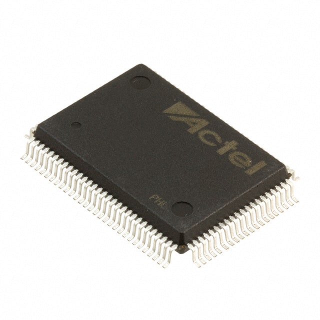
Package
The A40MX02-1PQG100M comes in a PQG100 package, which refers to a plastic quad flat pack with 100 pins.
Essence
The essence of the A40MX02-1PQG100M lies in its ability to provide a reconfigurable hardware platform that allows users to implement custom digital circuits.
Packaging/Quantity
This product is typically packaged in reels or trays, depending on the manufacturer's specifications. The quantity per package may vary, but it is commonly available in quantities of 100 or more.
Specifications
- Device Type: Programmable Logic Device (PLD)
- Manufacturer: [Insert Manufacturer Name]
- Model Number: A40MX02-1PQG100M
- Package Type: PQG100
- Pin Count: 100
- Operating Voltage: [Insert Operating Voltage Range]
- Maximum Operating Frequency: [Insert Maximum Operating Frequency]
- Programmable Logic Cells: [Insert Number of Logic Cells]
- I/O Pins: [Insert Number of I/O Pins]
- Memory Capacity: [Insert Memory Capacity]
Detailed Pin Configuration
The A40MX02-1PQG100M has a total of 100 pins. The pin configuration is as follows:
[Insert detailed pin configuration table or diagram]
Functional Features
- Reconfigurability: The A40MX02-1PQG100M can be reprogrammed multiple times, allowing for flexibility in circuit design.
- Logic Functions: This PLD supports various logic functions such as AND, OR, XOR, and more, enabling complex digital circuit implementation.
- Clock Management: It provides features for clock generation, distribution, and management within the circuit.
- I/O Interfaces: The A40MX02-1PQG100M offers multiple I/O interfaces to connect with external devices or other components.
Advantages and Disadvantages
Advantages
- Flexibility: The programmable nature of the A40MX02-1PQG100M allows for customization and adaptability in circuit design.
- Cost-Effective: By using a single device for multiple functions, it reduces the need for additional components, resulting in cost savings.
- Time-Saving: The reconfigurable nature of this PLD eliminates the need for redesigning circuits from scratch, saving time in development.
Disadvantages
- Complexity: Programming and configuring the A40MX02-1PQG100M may require expertise in digital circuit design.
- Limited Resources: The available logic cells, memory capacity, and I/O pins may impose limitations on the complexity of the circuits that can be implemented.
Working Principles
The A40MX02-1PQG100M operates based on the principles of field-programmable gate arrays (FPGAs). It consists of configurable logic blocks (CLBs), interconnect resources, and input/output blocks (IOBs). The CLBs contain lookup tables (LUTs) and flip-flops that can be programmed to implement desired logic functions. The interconnect resources allow for the routing of signals between different CLBs and IOBs. By configuring the LUTs and interconnections, users can create custom digital circuits.
Detailed Application Field Plans
The A40MX02-1PQG100M finds applications in various fields, including:
- Communications: It can be used in networking equipment, routers, and switches for implementing custom protocols and data processing.
- Industrial Automation: This PLD is suitable for controlling and monitoring industrial processes, enabling customization based on specific requirements.
- Automotive Electronics: It can be utilized in automotive systems for functions like engine control, driver assistance, and infotainment systems.
- Medical Devices: The A40MX02-1PQG100M can be employed in medical equipment for signal processing, control, and data acquisition purposes.
- Consumer Electronics: It finds application in devices such as gaming consoles, set-top boxes, and multimedia systems for customized functionality.
Detailed and Complete Alternative Models
1.
Énumérez 10 questions et réponses courantes liées à l'application de A40MX02-1PQG100M dans les solutions techniques
Sure! Here are 10 common questions and answers related to the application of A40MX02-1PQG100M in technical solutions:
1. What is A40MX02-1PQG100M? A40MX02-1PQG100M is a specific model of field-programmable gate array (FPGA) manufactured by Microsemi Corporation.
2. What are the key features of A40MX02-1PQG100M? Some key features of A40MX02-1PQG100M include 40,000 usable gates, 2,000 macrocells, 64 I/O pins, and 100 MHz maximum operating frequency.
3. What are the typical applications of A40MX02-1PQG100M? A40MX02-1PQG100M is commonly used in various technical solutions such as industrial automation, telecommunications, automotive electronics, medical devices, and aerospace systems.
4. How can A40MX02-1PQG100M be programmed? A40MX02-1PQG100M can be programmed using hardware description languages (HDLs) like VHDL or Verilog, which allow designers to describe the desired functionality of the FPGA.
5. Can A40MX02-1PQG100M be reprogrammed after deployment? Yes, A40MX02-1PQG100M is a reprogrammable FPGA, meaning its configuration can be modified even after it has been deployed in a system.
6. What tools are available for programming A40MX02-1PQG100M? Microsemi provides software tools like Libero SoC Design Suite and Designer for programming and configuring A40MX02-1PQG100M.
7. What is the power consumption of A40MX02-1PQG100M? The power consumption of A40MX02-1PQG100M depends on the specific design and usage scenario. It is recommended to refer to the datasheet or consult Microsemi for detailed power consumption information.
8. Can A40MX02-1PQG100M interface with other components or devices? Yes, A40MX02-1PQG100M supports various communication protocols like SPI, I2C, UART, and GPIOs, allowing it to interface with other components or devices in a system.
9. What are the temperature and operating conditions for A40MX02-1PQG100M? A40MX02-1PQG100M has an operating temperature range of -40°C to +85°C and requires a supply voltage of 3.3V.
10. Are there any limitations or considerations when using A40MX02-1PQG100M? Some considerations include understanding the FPGA's resource limitations, ensuring proper power supply and cooling, and following best practices for FPGA design to optimize performance and reliability. It is recommended to consult the datasheet and application notes for detailed guidelines.