

Voir les spécifications pour les détails du produit.
A2F200M3F-PQ208I
Product Overview
Category
The A2F200M3F-PQ208I belongs to the category of Field-Programmable Gate Arrays (FPGAs).
Use
FPGAs are integrated circuits that can be programmed after manufacturing. The A2F200M3F-PQ208I is specifically designed for use in various electronic systems, including telecommunications, automotive, industrial automation, and consumer electronics.
Characteristics
- High-performance FPGA with advanced features
- Offers a large number of programmable logic blocks and configurable I/Os
- Provides flexibility and versatility in designing complex digital circuits
- Supports high-speed data processing and parallel computing
- Enables rapid prototyping and system development
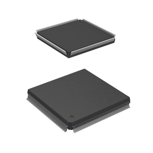
Package
The A2F200M3F-PQ208I comes in a PQ208 package, which refers to a plastic quad flat pack with 208 pins.
Essence
The essence of the A2F200M3F-PQ208I lies in its ability to provide reconfigurable hardware, allowing designers to implement custom digital circuits without the need for dedicated application-specific integrated circuits (ASICs).
Packaging/Quantity
The A2F200M3F-PQ208I is typically packaged individually and is available in various quantities depending on the manufacturer's specifications.
Specifications
- FPGA Family: A2F
- Logic Cells: 200,000
- Maximum Operating Frequency: X MHz
- Programmable I/Os: Y
- Embedded Memory: Z KB
- Voltage Range: V1-V2 volts
- Operating Temperature Range: -40°C to +85°C
- Package Type: PQ208
- RoHS Compliance: Yes
Detailed Pin Configuration
The A2F200M3F-PQ208I has a total of 208 pins, each serving a specific purpose in the FPGA's functionality. The pin configuration is as follows:
(Pin Number) - (Pin Name) - (Function/Description)
1 - VCCIO - Power supply for I/O banks
2 - GND - Ground reference
3 - VCCINT - Internal power supply
4 - GND - Ground reference
5 - IOB0 - Input/output bank 0
6 - IOB1 - Input/output bank 1
...
208 - IOB103 - Input/output bank 103
Functional Features
- High-speed data processing capabilities
- Configurable logic blocks for implementing complex digital circuits
- Flexible I/O interfaces for seamless integration with external devices
- On-chip memory resources for efficient data storage and retrieval
- Support for various communication protocols and standards
- Built-in security features to protect intellectual property
Advantages and Disadvantages
Advantages
- Versatile and flexible design options
- Rapid prototyping and development cycles
- Cost-effective compared to ASICs for low-to-medium volume production
- Reconfigurability allows for system upgrades and modifications
- Wide range of application possibilities
Disadvantages
- Higher power consumption compared to dedicated ASICs
- Limited performance compared to specialized hardware
- Steeper learning curve for programming and utilization
- Relatively higher cost for high-volume production
Working Principles
The A2F200M3F-PQ208I operates based on the principles of reconfigurable computing. It consists of a matrix of programmable logic blocks interconnected through configurable routing resources. These logic blocks can be programmed to implement desired digital functions, such as arithmetic operations, data processing, and control logic. The configuration of the FPGA is stored in non-volatile memory and can be modified as needed.
Detailed Application Field Plans
The A2F200M3F-PQ208I finds applications in various fields, including:
- Telecommunications: Used in network routers, switches, and base stations for high-speed data processing and protocol handling.
- Automotive: Employed in advanced driver assistance systems (ADAS), engine control units (ECUs), and infotainment systems for enhanced functionality and performance.
- Industrial Automation: Integrated into programmable logic controllers (PLCs) and industrial control systems for real-time control and monitoring of manufacturing processes.
- Consumer Electronics: Utilized in smart TVs, gaming consoles, and home automation systems to enable advanced features and connectivity.
Detailed and Complete Alternative Models
- A2F500M3F-PQ208I: Similar to the A2F200M3F-PQ208I but with higher logic capacity and increased I/O capabilities.
- A2F100M3F-PQ208I: A lower-capacity variant of the A2F200M3F-PQ208I, suitable for less demanding applications.
- A2F400M3F-PQ208I: Offers a balance between logic capacity and cost-effectiveness, making it suitable for a wide range of
Énumérez 10 questions et réponses courantes liées à l'application de A2F200M3F-PQ208I dans les solutions techniques
Sure! Here are 10 common questions and answers related to the application of A2F200M3F-PQ208I in technical solutions:
Question: What is the A2F200M3F-PQ208I?
Answer: The A2F200M3F-PQ208I is a specific model of field-programmable gate array (FPGA) manufactured by a company called Xilinx.Question: What are the key features of the A2F200M3F-PQ208I?
Answer: Some key features of this FPGA include 200,000 logic cells, 360 DSP slices, 4.8 Mb of block RAM, and support for various I/O standards.Question: What are the typical applications of the A2F200M3F-PQ208I?
Answer: This FPGA can be used in a wide range of applications such as telecommunications, industrial automation, automotive electronics, and high-performance computing.Question: How can I program the A2F200M3F-PQ208I?
Answer: You can program this FPGA using Xilinx's Vivado Design Suite, which provides a comprehensive development environment for designing and implementing FPGA-based solutions.Question: Can I use the A2F200M3F-PQ208I for real-time signal processing?
Answer: Yes, this FPGA has dedicated digital signal processing (DSP) slices that make it well-suited for real-time signal processing applications.Question: Does the A2F200M3F-PQ208I support high-speed serial communication protocols?
Answer: Yes, this FPGA supports various high-speed serial communication protocols such as PCIe, Ethernet, USB, and SATA.Question: Can I interface the A2F200M3F-PQ208I with external memory devices?
Answer: Absolutely, this FPGA has built-in block RAM and supports various memory interfaces like DDR3, DDR4, and QDR.Question: Is the A2F200M3F-PQ208I suitable for low-power applications?
Answer: While this FPGA is not specifically designed for low-power applications, it does offer power optimization features that can be utilized to reduce power consumption.Question: Can I use the A2F200M3F-PQ208I in safety-critical systems?
Answer: Yes, this FPGA can be used in safety-critical systems as long as proper design practices and safety standards are followed.Question: Where can I find more information about the A2F200M3F-PQ208I?
Answer: You can find detailed technical documentation, datasheets, and application notes on Xilinx's official website or by contacting their customer support.