

Voir les spécifications pour les détails du produit.
ATF22V10C-7JC
Product Overview
Category
ATF22V10C-7JC belongs to the category of programmable logic devices (PLDs).
Use
It is commonly used in digital circuit design and implementation, specifically for applications that require programmable logic functions.
Characteristics
- Programmable: The ATF22V10C-7JC can be programmed to perform various logic functions.
- Versatile: It offers a wide range of applications due to its programmability.
- High-speed operation: The device operates at a high clock frequency, enabling efficient processing of digital signals.
- Low power consumption: It is designed to consume minimal power during operation.
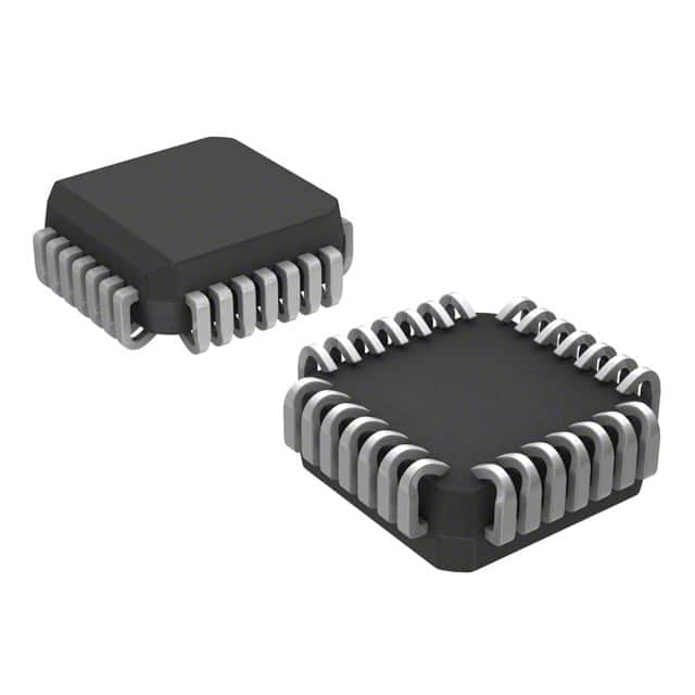
Package
The ATF22V10C-7JC is available in a compact 28-pin PLCC (Plastic Leaded Chip Carrier) package.
Essence
The essence of ATF22V10C-7JC lies in its ability to provide flexible and customizable logic functions, allowing designers to implement complex digital circuits efficiently.
Packaging/Quantity
The ATF22V10C-7JC is typically packaged in reels or tubes, with each reel/tube containing a specific quantity of devices. The exact packaging and quantity may vary depending on the supplier.
Specifications
- Operating Voltage: 5V
- Maximum Operating Frequency: 7 MHz
- Number of Inputs: 22
- Number of Outputs: 10
- Programmable Logic Cells: 22
- Maximum Propagation Delay: 15 ns
- Operating Temperature Range: -40°C to +85°C
Detailed Pin Configuration
The ATF22V10C-7JC features a total of 28 pins, each serving a specific purpose. Here is a detailed pin configuration:
- GND (Ground)
- I/O0 (Input/Output 0)
- I/O1 (Input/Output 1)
- I/O2 (Input/Output 2)
- I/O3 (Input/Output 3)
- I/O4 (Input/Output 4)
- I/O5 (Input/Output 5)
- I/O6 (Input/Output 6)
- I/O7 (Input/Output 7)
- I/O8 (Input/Output 8)
- I/O9 (Input/Output 9)
- VCC (Power Supply)
- /OE (Output Enable)
- /CE (Chip Enable)
- CLK (Clock Input)
- /PGM (Program Mode)
- /PRG (Program)
- /VPP (Programming Voltage)
- /ERASE (Erase)
- /RDY/BUSY (Ready/Busy)
- /RESET (Reset)
- /TEST (Test)
- NC (No Connection)
- NC (No Connection)
- NC (No Connection)
- NC (No Connection)
- NC (No Connection)
- NC (No Connection)
Functional Features
The ATF22V10C-7JC offers the following functional features:
- Programmable Logic Cells: The device contains 22 programmable logic cells, allowing for the implementation of various logic functions.
- Output Enable (/OE): This pin enables or disables the output of the device.
- Chip Enable (/CE): This pin activates or deactivates the device.
- Clock Input (CLK): The clock input synchronizes the operation of the device.
- Program Mode (/PGM): This pin sets the device in programming mode.
- Programming (/PRG): This pin initiates the programming process.
- Programming Voltage (/VPP): This pin provides the necessary voltage for programming.
- Erase (/ERASE): This pin erases the programmed logic cells.
- Ready/Busy (/RDY/BUSY): This pin indicates the status of the device (ready or busy).
- Reset (/RESET): This pin resets the device to its initial state.
- Test (/TEST): This pin is used for testing purposes.
Advantages and Disadvantages
Advantages
- Flexibility: The ATF22V10C-7JC offers flexibility in designing digital circuits due to its programmability.
- Cost-effective: It eliminates the need for custom-designed logic circuits, reducing overall costs.
- Time-saving: The device allows for quick prototyping and modifications without requiring physical changes to the circuitry.
- Compact size: The PLCC package ensures a compact form factor, making it suitable for space-constrained applications.
Disadvantages
- Limited complexity: The device may not be suitable for highly complex digital circuits that require a large number of logic functions.
- Programming expertise required: Proper programming knowledge is necessary to utilize the device effectively.
- Single-sourced: Availability from a single manufacturer may limit sourcing options.
Working Principles
The ATF22V10C-7JC
Énumérez 10 questions et réponses courantes liées à l'application de ATF22V10C-7JC dans les solutions techniques
Sure! Here are 10 common questions and answers related to the application of ATF22V10C-7JC in technical solutions:
Q: What is ATF22V10C-7JC? A: ATF22V10C-7JC is a programmable logic device (PLD) manufactured by Microchip Technology Inc.
Q: What is the purpose of ATF22V10C-7JC? A: ATF22V10C-7JC is used for implementing digital logic functions in various electronic systems and applications.
Q: What are the key features of ATF22V10C-7JC? A: Some key features include 22V10 architecture, 24-pin PLCC package, 10 macrocells, 7ns propagation delay, and JTAG boundary scan support.
Q: How can I program ATF22V10C-7JC? A: ATF22V10C-7JC can be programmed using industry-standard programming tools such as PALASM, ABEL, or VHDL.
Q: What is the maximum number of inputs and outputs supported by ATF22V10C-7JC? A: ATF22V10C-7JC supports up to 22 inputs and 10 outputs.
Q: Can ATF22V10C-7JC be reprogrammed after it has been programmed once? A: No, ATF22V10C-7JC is a one-time programmable device and cannot be reprogrammed.
Q: What are some typical applications of ATF22V10C-7JC? A: ATF22V10C-7JC is commonly used in applications such as memory decoding, address decoding, bus interfacing, and control logic implementation.
Q: What is the power supply voltage range for ATF22V10C-7JC? A: The recommended power supply voltage range for ATF22V10C-7JC is 4.5V to 5.5V.
Q: Can ATF22V10C-7JC operate in high-temperature environments? A: Yes, ATF22V10C-7JC has a specified operating temperature range of -40°C to +85°C, making it suitable for various industrial and automotive applications.
Q: Are there any design considerations when using ATF22V10C-7JC? A: Yes, some design considerations include proper decoupling capacitor placement, signal integrity, and ensuring that the device is correctly programmed according to the desired logic functions.
Please note that these answers are general and may vary depending on specific requirements and application scenarios.