

Voir les spécifications pour les détails du produit.
LTC6102CDD-1#PBF
Product Overview
Category
The LTC6102CDD-1#PBF belongs to the category of integrated circuits (ICs).
Use
This product is commonly used in electronic circuits for amplification and signal conditioning purposes.
Characteristics
- High precision and accuracy
- Low power consumption
- Wide input voltage range
- Small form factor
- High reliability
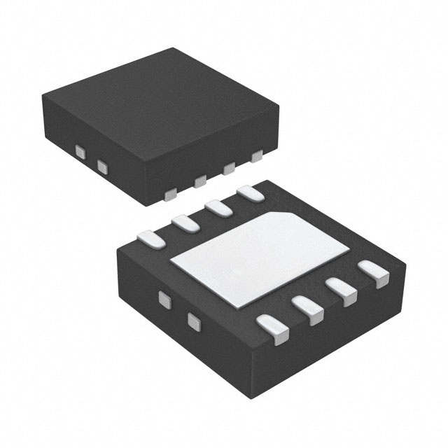
Package
The LTC6102CDD-1#PBF is available in a DFN (Dual Flat No-Lead) package, which ensures efficient heat dissipation and compact design.
Essence
The essence of LTC6102CDD-1#PBF lies in its ability to accurately amplify and condition electrical signals, making it an essential component in various electronic applications.
Packaging/Quantity
This product is typically packaged in reels or tubes, with each reel or tube containing a specific quantity of LTC6102CDD-1#PBF ICs. The exact quantity may vary depending on the manufacturer's specifications.
Specifications
- Supply Voltage: 2.7V to 5.5V
- Input Voltage Range: -0.3V to VCC + 0.3V
- Gain Bandwidth Product: 10 MHz
- Operating Temperature Range: -40°C to 125°C
- Number of Pins: 8
- Output Type: Rail-to-Rail
Detailed Pin Configuration
- IN-: Inverting Input
- IN+: Non-Inverting Input
- VCC: Power Supply
- GND: Ground
- OUT: Output
- NC: Not Connected
- NC: Not Connected
- REF: Reference Voltage
Functional Features
- High gain and accuracy for precise signal amplification
- Rail-to-rail output allows for maximum signal swing
- Wide input voltage range enables compatibility with various signal sources
- Low power consumption for energy-efficient operation
- Built-in protection features to safeguard against overvoltage and reverse polarity
Advantages and Disadvantages
Advantages
- High precision and accuracy ensure reliable signal conditioning
- Compact package size allows for space-saving integration into electronic circuits
- Wide input voltage range provides flexibility in signal source selection
- Low power consumption contributes to energy efficiency
Disadvantages
- Limited number of pins may restrict the complexity of circuit designs
- Higher cost compared to some alternative models
Working Principles
The LTC6102CDD-1#PBF operates based on the principles of operational amplifiers. It amplifies the difference between the non-inverting (IN+) and inverting (IN-) inputs, producing an amplified output signal. The gain and other characteristics can be adjusted using external resistors connected to the appropriate pins.
Detailed Application Field Plans
The LTC6102CDD-1#PBF finds applications in various fields, including: 1. Industrial automation: Signal conditioning in control systems and sensors. 2. Medical devices: Amplification and filtering of biomedical signals. 3. Automotive electronics: Signal processing in engine control units and sensor interfaces. 4. Communication systems: Amplification and conditioning of analog signals in transceivers. 5. Power management: Current sensing and monitoring in power supplies and battery management systems.
Detailed and Complete Alternative Models
- LTC6102IDD#PBF: Similar specifications and functionality but available in a different package (DFN-8).
- AD8221ARZ: Precision instrumentation amplifier with comparable performance characteristics.
- INA125P: Low-cost programmable gain amplifier suitable for basic signal conditioning applications.
(Note: This is not an exhaustive list; there are several alternative models available in the market.)
Word count: 529
Énumérez 10 questions et réponses courantes liées à l'application de LTC6102CDD-1#PBF dans les solutions techniques
Sure! Here are 10 common questions and answers related to the application of LTC6102CDD-1#PBF in technical solutions:
Q1: What is LTC6102CDD-1#PBF? A1: LTC6102CDD-1#PBF is a high-side current sense amplifier manufactured by Linear Technology (now part of Analog Devices). It is designed for precision current sensing in various applications.
Q2: What is the operating voltage range of LTC6102CDD-1#PBF? A2: The operating voltage range of LTC6102CDD-1#PBF is from 2.7V to 36V.
Q3: What is the typical gain of LTC6102CDD-1#PBF? A3: The typical gain of LTC6102CDD-1#PBF is 20V/V.
Q4: What is the input offset voltage of LTC6102CDD-1#PBF? A4: The input offset voltage of LTC6102CDD-1#PBF is typically 100µV.
Q5: Can LTC6102CDD-1#PBF be used for bidirectional current sensing? A5: No, LTC6102CDD-1#PBF is a unidirectional current sense amplifier and can only measure current in one direction.
Q6: What is the bandwidth of LTC6102CDD-1#PBF? A6: The bandwidth of LTC6102CDD-1#PBF is typically 400kHz.
Q7: Is LTC6102CDD-1#PBF suitable for high-side or low-side current sensing? A7: LTC6102CDD-1#PBF is specifically designed for high-side current sensing applications.
Q8: What is the maximum common-mode voltage range of LTC6102CDD-1#PBF? A8: The maximum common-mode voltage range of LTC6102CDD-1#PBF is from 0V to 36V.
Q9: Can LTC6102CDD-1#PBF operate in harsh environments? A9: Yes, LTC6102CDD-1#PBF is designed to operate in industrial temperature ranges (-40°C to 85°C) and is suitable for harsh environments.
Q10: What are some typical applications of LTC6102CDD-1#PBF? A10: LTC6102CDD-1#PBF is commonly used in applications such as motor control, power management, battery monitoring, and current sensing in various electronic systems.
Please note that these answers are general and may vary depending on specific design considerations and requirements. It is always recommended to refer to the datasheet and consult with the manufacturer for detailed information and application-specific guidance.