

Voir les spécifications pour les détails du produit.
LTC2612CMS8#TRPBF
Product Overview
- Category: Digital-to-Analog Converter (DAC)
- Use: LTC2612CMS8#TRPBF is a high-performance DAC designed for precision applications.
- Characteristics:
- High accuracy and resolution
- Low power consumption
- Small package size
- Wide temperature range
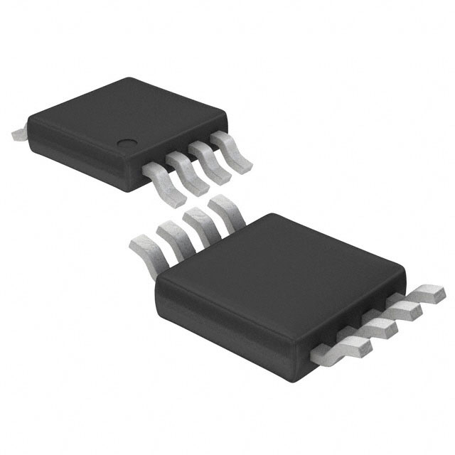
- Package: MSOP-8
- Essence: LTC2612CMS8#TRPBF is an essential component in systems requiring accurate analog voltage generation.
- Packaging/Quantity: The product is typically sold in reels of 2500 units.
Specifications
- Resolution: 16 bits
- Number of Channels: 1
- Output Type: Voltage
- Interface: Serial, SPI-compatible
- Supply Voltage Range: 2.7V to 5.5V
- Power Consumption: 0.6mW (typical)
- Temperature Range: -40°C to +85°C
Pin Configuration
The LTC2612CMS8#TRPBF has the following pin configuration:
```
| | | LTC2612CMS8 | |_______________________________________| | | | PIN CONFIGURATION | |_______________________________________| | | | 1 2 3 4 | | VDD CS SCK SDI | | | |_______________________________________| ```
Functional Features
- High accuracy: The LTC2612CMS8#TRPBF provides precise voltage outputs with its 16-bit resolution.
- Low power consumption: It consumes only 0.6mW of power, making it suitable for battery-powered devices.
- Serial interface: The DAC can be easily controlled using a serial peripheral interface (SPI).
- Wide temperature range: The LTC2612CMS8#TRPBF operates reliably in a wide temperature range, making it suitable for various environments.
Advantages and Disadvantages
Advantages: - High accuracy and resolution - Low power consumption - Small package size - Wide temperature range
Disadvantages: - Limited to single-channel output
Working Principles
The LTC2612CMS8#TRPBF utilizes a digital-to-analog conversion technique to convert digital input codes into precise analog voltage outputs. It employs an internal reference voltage and a resistor ladder network to achieve high accuracy and resolution.
Detailed Application Field Plans
The LTC2612CMS8#TRPBF is commonly used in the following applications: 1. Precision instrumentation 2. Data acquisition systems 3. Industrial control systems 4. Audio equipment 5. Test and measurement equipment
Alternative Models
Here are some alternative models that can be considered as alternatives to LTC2612CMS8#TRPBF: 1. AD5621RBRMZ-RL7 by Analog Devices 2. MCP4921-E/P by Microchip Technology 3. MAX5216EUB+T by Maxim Integrated
These models offer similar functionality and performance characteristics to LTC2612CMS8#TRPBF and can be used as drop-in replacements in many applications.
In conclusion, LTC2612CMS8#TRPBF is a high-performance DAC with excellent accuracy and resolution. Its low power consumption, small package size, and wide temperature range make it suitable for various precision applications.
Énumérez 10 questions et réponses courantes liées à l'application de LTC2612CMS8#TRPBF dans les solutions techniques
Sure! Here are 10 common questions and answers related to the application of LTC2612CMS8#TRPBF in technical solutions:
Q: What is LTC2612CMS8#TRPBF? A: LTC2612CMS8#TRPBF is a specific model number for a digital-to-analog converter (DAC) chip manufactured by Linear Technology (now part of Analog Devices).
Q: What is the purpose of LTC2612CMS8#TRPBF? A: The purpose of LTC2612CMS8#TRPBF is to convert digital signals into analog voltages, making it useful in various applications such as audio systems, instrumentation, and control systems.
Q: What is the resolution of LTC2612CMS8#TRPBF? A: LTC2612CMS8#TRPBF has a resolution of 12 bits, meaning it can represent analog voltages with a precision of 1 part in 4096.
Q: What is the operating voltage range of LTC2612CMS8#TRPBF? A: LTC2612CMS8#TRPBF operates from a single power supply voltage ranging from 2.7V to 5.5V.
Q: How many channels does LTC2612CMS8#TRPBF have? A: LTC2612CMS8#TRPBF is a dual-channel DAC, which means it can generate two independent analog output voltages simultaneously.
Q: What is the output voltage range of LTC2612CMS8#TRPBF? A: The output voltage range of LTC2612CMS8#TRPBF is determined by the reference voltage provided to the chip. It can be set between 0V and the reference voltage.
Q: Can LTC2612CMS8#TRPBF be controlled digitally? A: Yes, LTC2612CMS8#TRPBF can be controlled using a digital interface such as I2C or SPI, allowing for easy integration with microcontrollers or other digital systems.
Q: Does LTC2612CMS8#TRPBF have any built-in features for signal conditioning? A: Yes, LTC2612CMS8#TRPBF includes a programmable output range and an internal reference voltage, which can be used for signal conditioning purposes.
Q: What is the typical settling time of LTC2612CMS8#TRPBF? A: The settling time of LTC2612CMS8#TRPBF depends on various factors such as the applied voltage and load conditions. Typically, it ranges from a few microseconds to tens of microseconds.
Q: Is LTC2612CMS8#TRPBF suitable for precision applications? A: Yes, LTC2612CMS8#TRPBF is designed for precision applications, offering low integral non-linearity (INL) and differential non-linearity (DNL) specifications, ensuring accurate analog output voltages.
Please note that the answers provided here are general and may vary depending on specific datasheet information and application requirements.