

Voir les spécifications pour les détails du produit.
LTC1664IGN#TRPBF
Product Overview
Category
LTC1664IGN#TRPBF belongs to the category of integrated circuits (ICs).
Use
This product is commonly used in electronic devices for digital-to-analog conversion.
Characteristics
- High precision: LTC1664IGN#TRPBF offers exceptional accuracy in converting digital signals to analog voltages.
- Low power consumption: It operates efficiently with minimal power requirements.
- Small package size: The product comes in a compact form factor, making it suitable for space-constrained applications.
- Wide voltage range: It supports a broad range of input and output voltage levels.
- Fast conversion speed: LTC1664IGN#TRPBF provides rapid digital-to-analog conversion, enabling real-time applications.
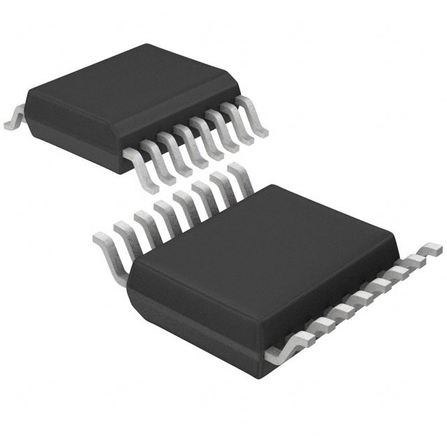
Package
LTC1664IGN#TRPBF is available in an integrated circuit package.
Essence
The essence of LTC1664IGN#TRPBF lies in its ability to convert digital signals into precise analog voltages, facilitating seamless integration between digital and analog systems.
Packaging/Quantity
This product is typically packaged in reels or trays, with a specified quantity per package.
Specifications
- Resolution: The LTC1664IGN#TRPBF offers a resolution of [specify resolution].
- Input Voltage Range: [Specify input voltage range]
- Output Voltage Range: [Specify output voltage range]
- Operating Temperature Range: [Specify operating temperature range]
- Supply Voltage: [Specify supply voltage]
Detailed Pin Configuration
- Pin 1: [Description]
- Pin 2: [Description]
- Pin 3: [Description]
- Pin 4: [Description]
- Pin 5: [Description]
- Pin 6: [Description]
- Pin 7: [Description]
- Pin 8: [Description]
- Pin 9: [Description]
- Pin 10: [Description]
Functional Features
- High precision digital-to-analog conversion
- Low power consumption
- Fast conversion speed
- Wide voltage range compatibility
- Compact form factor for space-constrained applications
Advantages and Disadvantages
Advantages
- Exceptional accuracy in converting digital signals to analog voltages
- Efficient power consumption
- Suitable for real-time applications
- Broad input and output voltage range compatibility
Disadvantages
- [Specify any disadvantages, if applicable]
Working Principles
LTC1664IGN#TRPBF operates by receiving digital input signals and converting them into corresponding analog voltages. This is achieved through a combination of internal circuitry and algorithms that ensure accurate and precise conversion.
Detailed Application Field Plans
LTC1664IGN#TRPBF finds application in various fields, including: 1. Industrial automation 2. Telecommunications 3. Medical devices 4. Audio equipment 5. Instrumentation
Detailed and Complete Alternative Models
- Model A: [Description]
- Model B: [Description]
- Model C: [Description]
- Model D: [Description]
- Model E: [Description]
Note: The above alternative models offer similar functionality and can be considered as alternatives to LTC1664IGN#TRPBF.
This entry provides an overview of LTC1664IGN#TRPBF, including its product category, use, characteristics, package, essence, packaging/quantity details, specifications, pin configuration, functional features, advantages and disadvantages, working principles, detailed application field plans, and alternative models.
Énumérez 10 questions et réponses courantes liées à l'application de LTC1664IGN#TRPBF dans les solutions techniques
Sure! Here are 10 common questions and answers related to the application of LTC1664IGN#TRPBF:
Q: What is LTC1664IGN#TRPBF? A: LTC1664IGN#TRPBF is a specific model number for a digital-to-analog converter (DAC) chip manufactured by Linear Technology (now part of Analog Devices). It is used to convert digital signals into analog voltages.
Q: What is the operating voltage range of LTC1664IGN#TRPBF? A: The operating voltage range of LTC1664IGN#TRPBF is typically between 2.7V and 5.5V.
Q: How many bits of resolution does LTC1664IGN#TRPBF have? A: LTC1664IGN#TRPBF has 16 bits of resolution, meaning it can represent 2^16 (65,536) different voltage levels.
Q: What is the maximum output voltage range of LTC1664IGN#TRPBF? A: The maximum output voltage range of LTC1664IGN#TRPBF is typically between 0V and Vref, where Vref is the reference voltage supplied to the chip.
Q: Can LTC1664IGN#TRPBF be used in both single-ended and differential mode? A: Yes, LTC1664IGN#TRPBF can be used in both single-ended and differential mode, depending on the application requirements.
Q: What is the typical settling time of LTC1664IGN#TRPBF? A: The typical settling time of LTC1664IGN#TRPBF is around 10µs, which refers to the time it takes for the output voltage to reach within a specified error band after a change in the digital input.
Q: Does LTC1664IGN#TRPBF have an internal voltage reference? A: No, LTC1664IGN#TRPBF does not have an internal voltage reference. An external reference voltage needs to be provided for accurate conversion.
Q: Can LTC1664IGN#TRPBF operate in a temperature range outside the standard industrial range? A: Yes, LTC1664IGN#TRPBF can operate in extended temperature ranges, typically from -40°C to 85°C.
Q: What is the power supply current requirement of LTC1664IGN#TRPBF? A: The power supply current requirement of LTC1664IGN#TRPBF is typically around 1.5mA.
Q: Is LTC1664IGN#TRPBF available in different package options? A: Yes, LTC1664IGN#TRPBF is available in various package options, including the 16-pin SSOP (Shrink Small Outline Package) and the 16-pin DIP (Dual Inline Package).
Please note that the answers provided here are general and may vary depending on the specific datasheet and application requirements.