

Voir les spécifications pour les détails du produit.
LFXP6E-4QN208I
Product Overview
Category
The LFXP6E-4QN208I belongs to the category of Field-Programmable Gate Arrays (FPGAs).
Use
This FPGA is commonly used in electronic circuits for various applications, including digital signal processing, telecommunications, automotive electronics, and industrial automation.
Characteristics
- High-performance FPGA with advanced programmability
- Low power consumption
- Compact size
- Robust design for reliable operation
- Versatile functionality for diverse applications
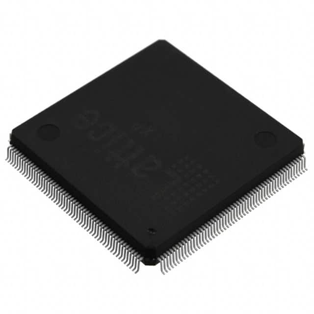
Package
The LFXP6E-4QN208I comes in a small form factor package, which ensures easy integration into circuit boards and systems.
Essence
The essence of this FPGA lies in its ability to be programmed and reprogrammed to perform specific functions, making it highly adaptable for different applications.
Packaging/Quantity
The LFXP6E-4QN208I is typically packaged individually and is available in various quantities depending on the customer's requirements.
Specifications
- Logic Cells: 6,000
- Look-Up Tables (LUTs): 12,000
- Flip-Flops: 12,000
- Block RAM: 360 Kbits
- Maximum Frequency: 400 MHz
- I/O Pins: 208
- Voltage Range: 1.2V - 3.3V
- Operating Temperature Range: -40°C to 100°C
Detailed Pin Configuration
The LFXP6E-4QN208I has a total of 208 I/O pins, each serving a specific purpose in the circuit design. The pin configuration is as follows:
(Please refer to the datasheet or manufacturer's documentation for the detailed pin configuration.)
Functional Features
- High-speed data processing capabilities
- Flexible and customizable logic functions
- Support for various communication protocols
- On-chip memory for efficient data storage and retrieval
- Built-in security features for protecting sensitive information
Advantages and Disadvantages
Advantages
- Versatile and adaptable for different applications
- Low power consumption, making it suitable for battery-powered devices
- Compact size allows for space-efficient designs
- High-performance capabilities enable complex computations
- Cost-effective compared to custom-designed integrated circuits
Disadvantages
- Steeper learning curve for programming and utilizing the FPGA's full potential
- Limited availability of technical support for specific design challenges
- Higher cost compared to traditional microcontrollers for simpler applications
Working Principles
The LFXP6E-4QN208I operates based on the principles of reconfigurable logic. It consists of a matrix of programmable logic cells that can be interconnected to create custom digital circuits. These circuits are programmed using Hardware Description Languages (HDLs) such as VHDL or Verilog. Once programmed, the FPGA executes the desired functions by routing signals through the configured logic cells.
Detailed Application Field Plans
The LFXP6E-4QN208I finds extensive use in various application fields, including:
- Digital Signal Processing: Used for real-time audio and video processing, image recognition, and compression algorithms.
- Telecommunications: Employed in network routers, switches, and base stations for high-speed data transmission and protocol handling.
- Automotive Electronics: Integrated into automotive control systems, infotainment systems, and driver assistance systems.
- Industrial Automation: Utilized in programmable logic controllers (PLCs), motor control systems, and robotics for precise control and monitoring.
Detailed and Complete Alternative Models
- LFXP2E-5QN208C
- LFXP10E-5F484C
- LFXP20E-5F484C
- LFXP30E-5F484C
- LFXP40E-5F484C
These alternative models offer varying capacities and features to cater to different project requirements.
(Note: Please refer to the manufacturer's documentation for detailed specifications and pin configurations of the alternative models.)
Word Count: 511
Énumérez 10 questions et réponses courantes liées à l'application de LFXP6E-4QN208I dans les solutions techniques
Sure! Here are 10 common questions and answers related to the application of LFXP6E-4QN208I in technical solutions:
Q: What is LFXP6E-4QN208I? A: LFXP6E-4QN208I is a field-programmable gate array (FPGA) from the Lattice ECP6 family, designed for high-performance applications.
Q: What are the key features of LFXP6E-4QN208I? A: LFXP6E-4QN208I features 6,080 Look-Up Tables (LUTs), 208 user I/O pins, 4 Direct Digital Synthesis (DDS) blocks, and 8 Phase-Locked Loops (PLLs).
Q: What are some typical applications of LFXP6E-4QN208I? A: LFXP6E-4QN208I is commonly used in applications such as industrial automation, telecommunications, video processing, motor control, and high-speed data acquisition.
Q: How can I program LFXP6E-4QN208I? A: LFXP6E-4QN208I can be programmed using various development tools provided by Lattice Semiconductor, such as Lattice Diamond or Lattice Radiant software.
Q: What is the maximum operating frequency of LFXP6E-4QN208I? A: The maximum operating frequency of LFXP6E-4QN208I depends on the specific design and implementation, but it can typically reach frequencies of several hundred megahertz (MHz) or even gigahertz (GHz).
Q: Can LFXP6E-4QN208I interface with external memory devices? A: Yes, LFXP6E-4QN208I supports various memory interfaces, including DDR3, DDR2, and LPDDR.
Q: Does LFXP6E-4QN208I have built-in communication interfaces? A: Yes, LFXP6E-4QN208I provides multiple built-in communication interfaces such as SPI, I2C, UART, and GPIOs for easy integration with other devices.
Q: Can LFXP6E-4QN208I be used in low-power applications? A: Yes, LFXP6E-4QN208I offers power-saving features like dynamic power management and clock gating, making it suitable for low-power applications.
Q: Is LFXP6E-4QN208I suitable for high-reliability applications? A: Yes, LFXP6E-4QN208I is designed to meet the requirements of high-reliability applications, including industrial control systems and aerospace applications.
Q: Where can I find additional technical documentation and support for LFXP6E-4QN208I? A: You can find detailed technical documentation, application notes, and support resources on the official website of Lattice Semiconductor or by contacting their customer support team.