

Voir les spécifications pour les détails du produit.
LFXP2-5E-5FTN256I
Product Overview
Category
The LFXP2-5E-5FTN256I belongs to the category of Field-Programmable Gate Arrays (FPGAs).
Use
FPGAs are integrated circuits that can be programmed and reprogrammed to perform various digital functions. The LFXP2-5E-5FTN256I is specifically designed for applications requiring high-performance and low-power consumption.
Characteristics
- High-performance FPGA with low power consumption
- Programmable and reprogrammable functionality
- Suitable for a wide range of applications
- Compact package size
- Robust and reliable design
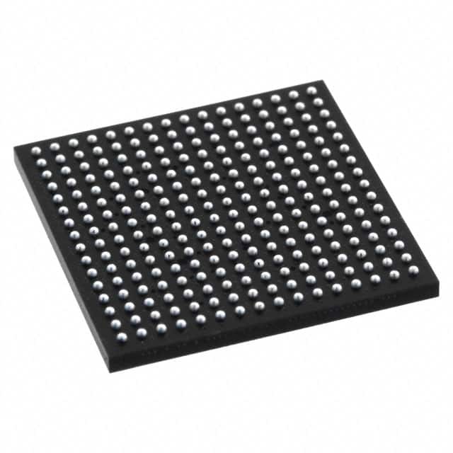
Package
The LFXP2-5E-5FTN256I comes in a compact package, ensuring easy integration into electronic systems. The package provides protection against environmental factors such as moisture and dust.
Essence
The essence of the LFXP2-5E-5FTN256I lies in its ability to provide flexible and customizable digital logic functions. It allows designers to implement complex algorithms and logic circuits without the need for custom-designed integrated circuits.
Packaging/Quantity
The LFXP2-5E-5FTN256I is typically packaged individually and is available in various quantities depending on the requirements of the application.
Specifications
- FPGA Family: LatticeXP2
- Logic Cells: 5,120
- Number of I/Os: 256
- Operating Voltage: 1.2V
- Maximum Frequency: 400 MHz
- Configuration Memory: Flash-based
- Package Type: 256-ball FineLine BGA
Detailed Pin Configuration
The LFXP2-5E-5FTN256I has a total of 256 pins, each serving a specific purpose in the FPGA's operation. The pin configuration includes input/output pins, power supply pins, clock pins, and configuration pins. A detailed pinout diagram can be found in the product datasheet.
Functional Features
- High-performance digital logic processing
- Low power consumption
- Flexible and customizable functionality
- Flash-based configuration memory for easy reprogramming
- Support for various communication protocols
- On-chip memory resources for data storage
- Built-in security features for protecting intellectual property
Advantages and Disadvantages
Advantages
- Versatile and adaptable to a wide range of applications
- Lower development time compared to custom-designed integrated circuits
- Cost-effective solution for small to medium-scale production
- Easy reprogrammability allows for iterative design improvements
- Availability of development tools and support from the manufacturer
Disadvantages
- Limited performance compared to application-specific integrated circuits (ASICs)
- Higher power consumption compared to dedicated hardware solutions
- Complexity of programming and debugging FPGAs
- Higher cost per unit compared to mass-produced standard integrated circuits
Working Principles
The LFXP2-5E-5FTN256I operates based on the principles of configurable logic blocks (CLBs) and interconnect resources. CLBs consist of look-up tables, flip-flops, and other components that can be programmed to implement desired logic functions. Interconnect resources provide routing paths between different CLBs, allowing for the flow of data and control signals.
The FPGA is configured by loading a bitstream into its configuration memory, which determines the behavior of the logic elements and interconnections. Once configured, the FPGA performs the desired digital functions according to the programmed logic.
Detailed Application Field Plans
The LFXP2-5E-5FTN256I finds applications in various fields, including:
- Telecommunications: Used in base stations, routers, and network switches for high-speed data processing and protocol handling.
- Industrial Automation: Employed in control systems, motor drives, and robotics for real-time data processing and control algorithms.
- Medical Devices: Integrated into medical imaging equipment, patient monitoring systems, and diagnostic instruments for signal processing and data analysis.
- Aerospace and Defense: Utilized in radar systems, communication satellites, and avionics for high-performance signal processing and encryption.
- Automotive Electronics: Incorporated into advanced driver assistance systems (ADAS), infotainment systems, and engine control units for efficient data processing and control.
Detailed and Complete Alternative Models
- LFXP2-17E-6FTN256C
- LFXP2-30E-7FTN256I
- LFXP2-40E-8FTN256C
- LFXP2-70E-9FTN256I
- LFXP2-125E-10FTN256C
These alternative models offer varying levels of logic capacity, I/O count, and performance to cater to different application requirements.
In conclusion, the LFXP2-5
Énumérez 10 questions et réponses courantes liées à l'application de LFXP2-5E-5FTN256I dans les solutions techniques
Sure! Here are 10 common questions and answers related to the application of LFXP2-5E-5FTN256I in technical solutions:
Q: What is the LFXP2-5E-5FTN256I? A: The LFXP2-5E-5FTN256I is a low-power, small form-factor FPGA (Field-Programmable Gate Array) from Lattice Semiconductor.
Q: What are the key features of the LFXP2-5E-5FTN256I? A: The key features include 5,120 Look-Up Tables (LUTs), 256 I/O pins, low power consumption, and support for various interfaces like SPI, I2C, and UART.
Q: What are some typical applications of the LFXP2-5E-5FTN256I? A: The LFXP2-5E-5FTN256I is commonly used in applications such as industrial automation, automotive electronics, consumer electronics, and communication systems.
Q: How can I program the LFXP2-5E-5FTN256I? A: The LFXP2-5E-5FTN256I can be programmed using Lattice Diamond or Lattice Radiant software tools provided by Lattice Semiconductor.
Q: What is the power supply requirement for the LFXP2-5E-5FTN256I? A: The LFXP2-5E-5FTN256I operates at a voltage range of 1.14V to 1.26V, with a recommended core voltage of 1.2V.
Q: Can I use the LFXP2-5E-5FTN256I in a battery-powered device? A: Yes, the LFXP2-5E-5FTN256I is designed for low power consumption, making it suitable for battery-powered applications.
Q: Does the LFXP2-5E-5FTN256I support high-speed interfaces? A: Yes, the LFXP2-5E-5FTN256I supports various high-speed interfaces like DDR3, LVDS, and PCI Express.
Q: Can I use the LFXP2-5E-5FTN256I for real-time signal processing? A: Yes, the LFXP2-5E-5FTN256I's high-performance architecture makes it suitable for real-time signal processing applications.
Q: Are there any development boards available for the LFXP2-5E-5FTN256I? A: Yes, Lattice Semiconductor provides development boards like the LFXP2-EVN for easy prototyping and evaluation of the LFXP2-5E-5FTN256I.
Q: Where can I find technical documentation and support for the LFXP2-5E-5FTN256I? A: You can find technical documentation, datasheets, application notes, and support resources on the official website of Lattice Semiconductor or by contacting their customer support team.