

Voir les spécifications pour les détails du produit.
LFE2M50E-5FN672C
Product Overview
Category
The LFE2M50E-5FN672C belongs to the category of Field Programmable Gate Arrays (FPGAs).
Use
FPGAs are integrated circuits that can be programmed and reprogrammed to perform various digital functions. The LFE2M50E-5FN672C is specifically designed for applications requiring high-performance and low-power consumption.
Characteristics
- High-performance FPGA with low power consumption
- Flexible and reprogrammable design
- Suitable for a wide range of applications
- Compact package size
- Advanced features for efficient implementation
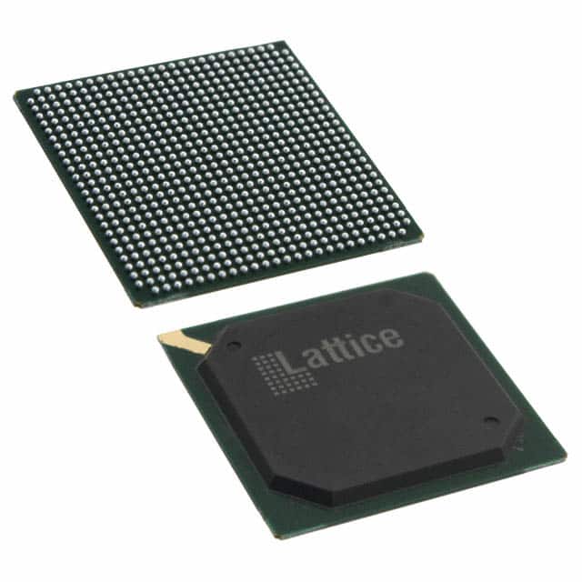
Package
The LFE2M50E-5FN672C comes in a compact package, which ensures easy integration into electronic systems. The package provides protection against environmental factors and facilitates efficient heat dissipation.
Essence
The essence of the LFE2M50E-5FN672C lies in its ability to provide a customizable digital logic solution for various applications. Its programmable nature allows for flexibility and adaptability, making it suitable for diverse projects.
Packaging/Quantity
The LFE2M50E-5FN672C is typically packaged individually and is available in various quantities depending on the requirements of the project or application.
Specifications
- FPGA Family: Lattice ECP2M
- Logic Elements: 50,000
- Number of I/Os: 672
- Operating Voltage: 1.2V
- Maximum Frequency: 400 MHz
- Embedded Memory: Up to 4.8 Mb
- Configuration Memory: 256 Kb
- Package Type: FineLine BGA
- Temperature Range: -40°C to +100°C
Detailed Pin Configuration
The LFE2M50E-5FN672C has a total of 672 pins, each serving a specific purpose. The pin configuration varies depending on the application and system requirements. For detailed pin assignments and configurations, please refer to the manufacturer's datasheet.
Functional Features
- High-performance digital logic implementation
- Low power consumption for energy-efficient operation
- Flexible and reprogrammable design for customization
- Advanced features for efficient resource utilization
- Support for various communication protocols and interfaces
- On-chip memory for data storage and processing
- Built-in security features for protecting sensitive information
Advantages and Disadvantages
Advantages
- Versatile and adaptable for a wide range of applications
- High-performance capabilities for demanding tasks
- Low power consumption for energy efficiency
- Compact package size for easy integration
- Cost-effective solution compared to custom ASIC designs
Disadvantages
- Steeper learning curve for programming and utilizing FPGA technology
- Limited availability of specialized technical support compared to mainstream technologies
- Higher cost compared to traditional microcontrollers for simple applications
Working Principles
The LFE2M50E-5FN672C operates based on the principles of field-programmable gate arrays. It consists of an array of configurable logic blocks interconnected through programmable routing resources. These logic blocks can be programmed to perform various digital functions, such as arithmetic operations, data processing, and control logic. The configuration of the FPGA is stored in non-volatile memory, allowing it to retain its functionality even after power cycles.
Detailed Application Field Plans
The LFE2M50E-5FN672C finds applications in various fields, including but not limited to:
- Telecommunications: Used in network infrastructure equipment for high-speed data processing and protocol handling.
- Industrial Automation: Employed in control systems for real-time monitoring and control of industrial processes.
- Automotive: Integrated into automotive electronics for advanced driver assistance systems (ADAS) and infotainment systems.
- Aerospace and Defense: Utilized in radar systems, avionics, and secure communication equipment.
- Medical Devices: Incorporated into medical imaging systems, patient monitoring devices, and laboratory equipment.
Detailed and Complete Alternative Models
- Xilinx Virtex-7 XC7VX485T FPGA
- Intel Cyclone V GX FPGA
- Microsemi SmartFusion2 SoC FPGA
- Altera MAX 10 FPGA
- QuickLogic EOS S3 FPGA
These alternative models offer similar functionality and performance to the LFE2M50E-5FN672C and can be considered as alternatives based on specific project requirements.
Word count: 550 words
Énumérez 10 questions et réponses courantes liées à l'application de LFE2M50E-5FN672C dans les solutions techniques
Sure! Here are 10 common questions and answers related to the application of LFE2M50E-5FN672C in technical solutions:
Q: What is the LFE2M50E-5FN672C? A: The LFE2M50E-5FN672C is a specific model of Field Programmable Gate Array (FPGA) manufactured by Lattice Semiconductor.
Q: What are the key features of the LFE2M50E-5FN672C? A: Some key features of this FPGA include 50,000 Look-Up Tables (LUTs), 672-pin FineLine BGA package, low power consumption, and high-speed performance.
Q: What are the typical applications of the LFE2M50E-5FN672C? A: This FPGA is commonly used in various technical solutions such as industrial automation, telecommunications, automotive electronics, medical devices, and more.
Q: How can I program the LFE2M50E-5FN672C? A: The LFE2M50E-5FN672C can be programmed using Lattice Diamond or Lattice Radiant software tools provided by Lattice Semiconductor.
Q: What is the maximum operating frequency of the LFE2M50E-5FN672C? A: The maximum operating frequency of this FPGA depends on the design and implementation, but it can typically reach frequencies of several hundred megahertz (MHz).
Q: Does the LFE2M50E-5FN672C support different I/O standards? A: Yes, this FPGA supports various I/O standards such as LVCMOS, LVTTL, SSTL, HSTL, LVDS, and more, making it versatile for different interface requirements.
Q: Can I use the LFE2M50E-5FN672C in a high-reliability application? A: Yes, this FPGA is designed to meet stringent quality and reliability standards, making it suitable for high-reliability applications such as aerospace or defense systems.
Q: What are the power supply requirements for the LFE2M50E-5FN672C? A: The LFE2M50E-5FN672C typically requires a single 3.3V power supply, but it also supports multiple power supply options for specific applications.
Q: Is the LFE2M50E-5FN672C compatible with other FPGA families from Lattice Semiconductor? A: Yes, the LFE2M50E-5FN672C is part of the Lattice ECP2M family, and it is compatible with other members of the same family, allowing for scalability and design reuse.
Q: Where can I find additional technical documentation and support for the LFE2M50E-5FN672C? A: You can find detailed technical documentation, datasheets, application notes, and support resources on the official website of Lattice Semiconductor or by contacting their customer support team.