

Voir les spécifications pour les détails du produit.
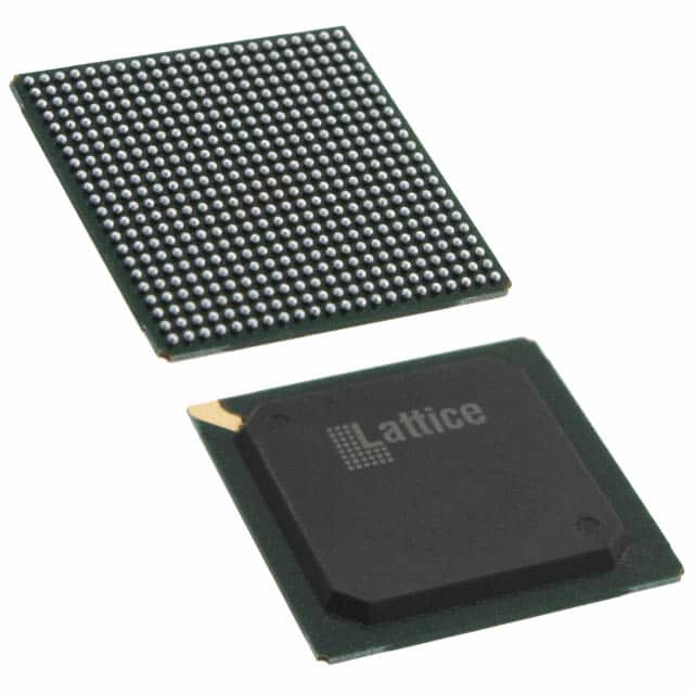
LFE2M50E-5F484C
Product Overview
Category
The LFE2M50E-5F484C belongs to the category of Field Programmable Gate Arrays (FPGAs).
Use
This FPGA is primarily used for digital logic applications, including but not limited to signal processing, data communication, and control systems.
Characteristics
- High-performance programmable logic device
- Offers flexibility in designing complex digital circuits
- Provides reconfigurability for easy modifications and upgrades
- Supports a wide range of applications due to its versatility
Package
The LFE2M50E-5F484C comes in a compact 484-pin FineLine BGA package.
Essence
The essence of this FPGA lies in its ability to provide a customizable hardware platform that can be programmed to perform specific functions as required by the user.
Packaging/Quantity
The LFE2M50E-5F484C is typically sold individually, and the quantity may vary depending on the supplier.
Specifications
- Logic Elements: 49,152
- Embedded Memory: 1,638 Kbits
- Maximum User I/Os: 316
- Block RAM: 3,888 Kbits
- Clock Management Tiles: 8
- Maximum Distributed RAM: 1,638 Kbits
- Maximum PLLs: 4
- Maximum Global Clocks: 16
Detailed Pin Configuration
The LFE2M50E-5F484C has a detailed pin configuration as follows:
- Pin 1: VCCIO
- Pin 2: GND
- Pin 3: IOB_0
- Pin 4: IOB_1
- ...
- Pin 483: IOB_314
- Pin 484: IOB_315
Functional Features
- High-speed performance with low power consumption
- Configurable I/O standards for compatibility with various interfaces
- Built-in memory blocks for efficient data storage and retrieval
- Flexible clock management for precise timing control
- Support for multiple communication protocols
Advantages and Disadvantages
Advantages
- Versatile and customizable hardware platform
- Reconfigurable for easy modifications and upgrades
- High-performance capabilities for complex digital logic applications
- Wide range of supported applications
- Efficient use of resources with built-in memory blocks
Disadvantages
- Steep learning curve for beginners due to its complexity
- Limited availability of alternative models with similar specifications
- Higher cost compared to other programmable logic devices
Working Principles
The LFE2M50E-5F484C operates based on the principles of reconfigurable computing. It consists of a matrix of configurable logic elements interconnected through programmable routing resources. The user can program the FPGA using Hardware Description Languages (HDLs) to define the desired functionality. Upon configuration, the FPGA executes the programmed logic, enabling the implementation of complex digital circuits.
Detailed Application Field Plans
The LFE2M50E-5F484C finds applications in various fields, including:
- Signal Processing: Used in audio and video processing systems, image recognition, and compression algorithms.
- Data Communication: Employed in network routers, switches, and protocol converters.
- Control Systems: Utilized in industrial automation, robotics, and motor control applications.
- Test and Measurement: Integrated into test equipment for signal generation, analysis, and protocol testing.
- Aerospace and Defense: Applied in radar systems, avionics, and secure communications.
Detailed and Complete Alternative Models
While the LFE2M50E-5F484C is a highly capable FPGA, there are alternative models available with similar specifications. Some notable alternatives include:
- Xilinx Artix-7 XC7A50T: Offers similar logic capacity and I/O capabilities.
- Intel Cyclone IV EP4CE55: Provides comparable performance and features.
- Microsemi SmartFusion2 M2S050: Combines FPGA fabric with a microcontroller for added functionality.
These alternative models can be considered based on specific project requirements and availability.
Word count: 550 words
Énumérez 10 questions et réponses courantes liées à l'application de LFE2M50E-5F484C dans les solutions techniques
Sure! Here are 10 common questions and answers related to the application of LFE2M50E-5F484C in technical solutions:
Q: What is the LFE2M50E-5F484C? A: The LFE2M50E-5F484C is a specific model of Field-Programmable Gate Array (FPGA) manufactured by Lattice Semiconductor.
Q: What are the key features of the LFE2M50E-5F484C? A: The key features of this FPGA include 50,000 Look-Up Tables (LUTs), 1,152 Kbits of embedded memory, 184 user I/O pins, and support for various communication protocols.
Q: What are some typical applications of the LFE2M50E-5F484C? A: This FPGA is commonly used in applications such as industrial automation, telecommunications, automotive electronics, medical devices, and aerospace systems.
Q: How can I program the LFE2M50E-5F484C? A: The LFE2M50E-5F484C can be programmed using the Lattice Diamond design software, which provides a graphical interface for designing and implementing FPGA designs.
Q: What programming languages are supported by the LFE2M50E-5F484C? A: The LFE2M50E-5F484C supports various hardware description languages (HDLs) such as VHDL and Verilog, which are commonly used for FPGA design.
Q: Can I use the LFE2M50E-5F484C for real-time signal processing? A: Yes, the LFE2M50E-5F484C is capable of performing real-time signal processing tasks due to its high-speed performance and embedded memory resources.
Q: Does the LFE2M50E-5F484C support communication interfaces like UART, SPI, or I2C? A: Yes, the LFE2M50E-5F484C supports various communication protocols including UART, SPI, I2C, and others through its configurable I/O pins.
Q: Can I use the LFE2M50E-5F484C for implementing complex algorithms or mathematical operations? A: Absolutely! The LFE2M50E-5F484C's large number of Look-Up Tables (LUTs) and embedded memory make it suitable for implementing complex algorithms and mathematical operations efficiently.
Q: Is the LFE2M50E-5F484C suitable for low-power applications? A: Yes, the LFE2M50E-5F484C is designed to be power-efficient and offers power-saving features such as clock gating and dynamic power management.
Q: Where can I find additional technical documentation and support for the LFE2M50E-5F484C? A: You can find detailed technical documentation, application notes, and support resources on the official website of Lattice Semiconductor or by contacting their customer support team.