

Voir les spécifications pour les détails du produit.
LFE2M35SE-6FN672C
Product Overview
Category
The LFE2M35SE-6FN672C belongs to the category of Field Programmable Gate Arrays (FPGAs).
Use
This FPGA is commonly used in various electronic devices and systems for digital logic implementation, such as communication equipment, industrial control systems, and consumer electronics.
Characteristics
- High-performance programmable logic device
- Offers flexibility and reconfigurability
- Provides a large number of configurable logic blocks (CLBs) and programmable interconnects
- Supports complex digital designs and algorithms
- Enables rapid prototyping and development cycles
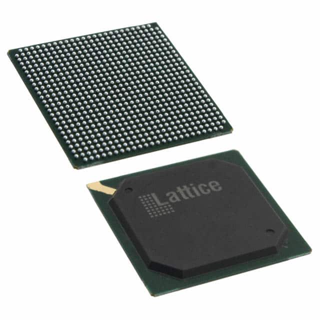
Package
The LFE2M35SE-6FN672C comes in a compact and durable package suitable for surface mount technology (SMT) assembly. The package ensures reliable electrical connections and protection against environmental factors.
Essence
The essence of the LFE2M35SE-6FN672C lies in its ability to provide a customizable hardware platform that can be programmed to perform specific functions according to the requirements of the application.
Packaging/Quantity
The LFE2M35SE-6FN672C is typically packaged in reels or trays, depending on the manufacturer's specifications. The quantity per package may vary, but it is commonly available in quantities suitable for both small-scale and large-scale production.
Specifications
- FPGA Family: Lattice ECP2M
- Device Type: LFE2M35SE
- Logic Elements: 35,000
- Speed Grade: -6
- Number of I/O Pins: 672
- Operating Voltage: 1.2V
- Package Type: FineLine BGA (Ball Grid Array)
- Package Pin Count: 672
- Temperature Range: Commercial (0°C to 85°C)
Detailed Pin Configuration
The LFE2M35SE-6FN672C has a total of 672 pins, each serving a specific purpose in the FPGA's functionality. The pin configuration includes input/output pins, power supply pins, clock pins, and configuration pins. For a detailed pin configuration diagram, please refer to the manufacturer's datasheet.
Functional Features
- High-Speed Performance: The LFE2M35SE-6FN672C offers high-speed operation, allowing for efficient execution of complex digital designs and algorithms.
- Flexible Configuration: With its large number of configurable logic blocks (CLBs) and programmable interconnects, this FPGA provides flexibility in implementing various logic functions.
- Reconfigurability: The FPGA can be reprogrammed multiple times, enabling rapid prototyping and design iterations without the need for hardware changes.
- Low Power Consumption: The LFE2M35SE-6FN672C is designed to minimize power consumption, making it suitable for battery-powered devices and energy-efficient applications.
- Integrated Hard IP Cores: The FPGA incorporates pre-designed hard intellectual property (IP) cores, such as memory controllers and communication interfaces, which enhance system integration and reduce development time.
Advantages and Disadvantages
Advantages
- High-performance and flexibility
- Reconfigurable nature allows for quick design iterations
- Integration of hard IP cores reduces development effort
- Low power consumption for energy-efficient applications
Disadvantages
- Steep learning curve for beginners due to the complexity of FPGA programming
- Higher cost compared to fixed-function integrated circuits for low-volume production
Working Principles
The LFE2M35SE-6FN672C operates based on the principles of digital logic implementation using configurable logic blocks (CLBs) and programmable interconnects. These CLBs can be programmed to perform various logical operations, while the interconnects allow for the routing of signals between different CLBs. The FPGA's configuration memory stores the programming information, which can be modified to change the functionality of the device.
Detailed Application Field Plans
The LFE2M35SE-6FN672C finds applications in various fields, including:
- Communication Equipment: Used in network routers, switches, and wireless communication systems for high-speed data processing and protocol handling.
- Industrial Control Systems: Employed in programmable logic controllers (PLCs) and automation systems for real-time control and monitoring of industrial processes.
- Consumer Electronics: Integrated into smart TVs, gaming consoles, and multimedia devices for advanced signal processing and multimedia functionalities.
- Medical Devices: Utilized in medical imaging equipment, patient monitoring systems, and laboratory instruments for data acquisition and processing.
- Automotive Electronics: Incorporated in automotive control units, infotainment systems, and driver assistance systems for enhanced performance and connectivity.
Detailed and Complete Alternative Models
- Xilinx Virtex-7 XC7VX485T: A high-performance FPGA with 485,760 logic cells and 3
Énumérez 10 questions et réponses courantes liées à l'application de LFE2M35SE-6FN672C dans les solutions techniques
Sure! Here are 10 common questions and answers related to the application of LFE2M35SE-6FN672C in technical solutions:
Q: What is LFE2M35SE-6FN672C? A: LFE2M35SE-6FN672C is a specific model of Field-Programmable Gate Array (FPGA) manufactured by Lattice Semiconductor.
Q: What are the key features of LFE2M35SE-6FN672C? A: Some key features of LFE2M35SE-6FN672C include 35,000 Look-Up Tables (LUTs), 672-pin FineLine BGA package, and support for various I/O standards.
Q: What are the typical applications of LFE2M35SE-6FN672C? A: LFE2M35SE-6FN672C is commonly used in applications such as industrial automation, telecommunications, automotive electronics, and medical devices.
Q: How can LFE2M35SE-6FN672C be programmed? A: LFE2M35SE-6FN672C can be programmed using the Lattice Diamond design software or other compatible programming tools.
Q: What are the power requirements for LFE2M35SE-6FN672C? A: The power supply voltage for LFE2M35SE-6FN672C is typically 1.2V, but it also supports other voltages depending on the specific application.
Q: Can LFE2M35SE-6FN672C interface with external devices? A: Yes, LFE2M35SE-6FN672C has various I/O standards and can interface with external devices such as sensors, memory modules, and communication interfaces.
Q: Is LFE2M35SE-6FN672C suitable for high-speed applications? A: Yes, LFE2M35SE-6FN672C supports high-speed interfaces and can be used in applications that require fast data processing or high-frequency signal handling.
Q: Can LFE2M35SE-6FN672C be reprogrammed after deployment? A: Yes, LFE2M35SE-6FN672C is a reprogrammable FPGA, allowing for updates or modifications to the design even after it has been deployed in a system.
Q: Are there any development boards available for LFE2M35SE-6FN672C? A: Yes, Lattice Semiconductor offers development boards specifically designed for LFE2M35SE-6FN672C, which provide a convenient platform for prototyping and testing.
Q: Where can I find more information about LFE2M35SE-6FN672C? A: You can find detailed technical documentation, datasheets, and application notes on the official website of Lattice Semiconductor or by contacting their support team.