

Voir les spécifications pour les détails du produit.
LCMXO256C-4M100C
Product Overview
Category: Programmable Logic Device (PLD)
Use: The LCMXO256C-4M100C is a high-performance PLD designed for various digital logic applications. It offers flexibility and versatility in implementing complex logic functions.
Characteristics: - Low power consumption - High-speed performance - Small form factor - Easy programmability - Wide range of I/O options
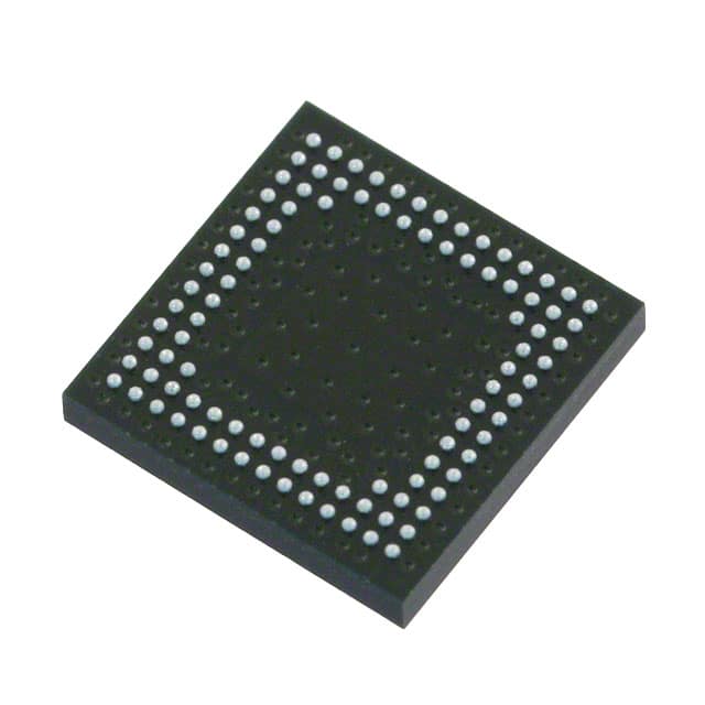
Package: The LCMXO256C-4M100C comes in a compact 100-pin Quad Flat No-Lead (QFN) package, which allows for easy integration into circuit boards.
Essence: This PLD provides designers with a cost-effective solution for implementing custom logic functions in a wide range of applications.
Packaging/Quantity: The LCMXO256C-4M100C is typically sold in reels or trays, with quantities varying based on customer requirements.
Specifications
- Logic Cells: 256
- Macrocells: 192
- I/O Pins: 100
- Operating Voltage: 1.2V
- Operating Temperature Range: -40°C to 85°C
- Maximum Frequency: 100MHz
- Programmable Logic Blocks: 32
- Embedded Memory: 4Kbits
- JTAG Boundary Scan Support: Yes
Detailed Pin Configuration
The LCMXO256C-4M100C has a total of 100 pins, each serving a specific purpose. Here are some of the key pin functions:
- VCCIO: Power supply voltage for I/O pins
- GND: Ground reference
- JTAGTMS, JTAGTCK, JTAGTDI, JTAGTDO: Pins for JTAG boundary scan support
- IO[0:99]: General-purpose I/O pins
- VCCINT: Power supply voltage for internal logic
For a complete pin configuration diagram, please refer to the product datasheet.
Functional Features
- Programmable Logic: The LCMXO256C-4M100C offers a wide range of programmable logic resources, allowing designers to implement complex logic functions.
- Embedded Memory: With 4Kbits of embedded memory, this PLD can store data and configuration information.
- I/O Flexibility: The device provides 100 I/O pins, enabling easy interfacing with external devices.
- Low Power Consumption: The LCMXO256C-4M100C is designed to operate at low power levels, making it suitable for battery-powered applications.
Advantages and Disadvantages
Advantages: - Versatile and flexible programmability - Compact form factor - Low power consumption - Wide operating temperature range - Cost-effective solution for custom logic implementation
Disadvantages: - Limited number of logic cells compared to higher-end PLDs - Maximum frequency limitation of 100MHz
Working Principles
The LCMXO256C-4M100C utilizes a combination of look-up tables (LUTs), flip-flops, and interconnect resources to implement user-defined logic functions. The device is programmed using hardware description languages (HDL) or schematic entry tools, which generate a configuration bitstream. This bitstream is then loaded into the PLD, configuring it to perform the desired logic operations.
Detailed Application Field Plans
The LCMXO256C-4M100C finds applications in various fields, including:
- Embedded Systems: It can be used to implement control and interface logic in embedded systems, such as industrial automation, robotics, and IoT devices.
- Communications: The PLD can be employed in communication systems for protocol conversion, data routing, and signal processing.
- Consumer Electronics: It can be utilized in consumer electronics products like gaming consoles, set-top boxes, and audio/video equipment for custom logic implementation.
- Automotive: The LCMXO256C-4M100C can be integrated into automotive systems for functions like engine control, driver assistance, and infotainment.
Detailed and Complete Alternative Models
- LCMXO2-1200ZE-1MG132C: This PLD offers a higher logic capacity and more I/O pins compared to the LCMXO256C-4M100C.
- LCMXO640C-4FTN256C: This PLD provides a lower logic capacity but operates at a higher maximum frequency.
- LCMXO2280C-4FTN324C: With a larger number of logic cells and I/O pins, this PLD is suitable for more complex applications.
These alternative models offer different trade-offs in terms of logic capacity, I/O options, and performance, allowing designers to choose the most suitable option for their specific requirements.
Énumérez 10 questions et réponses courantes liées à l'application de LCMXO256C-4M100C dans les solutions techniques
Sure! Here are 10 common questions and answers related to the application of LCMXO256C-4M100C in technical solutions:
Question: What is the LCMXO256C-4M100C?
Answer: The LCMXO256C-4M100C is a low-cost, low-power FPGA (Field-Programmable Gate Array) device manufactured by Lattice Semiconductor.Question: What are the key features of the LCMXO256C-4M100C?
Answer: Some key features include 256 LUTs (Look-Up Tables), 4,000 logic cells, 100 MHz maximum operating frequency, and 4 Mbit embedded flash memory.Question: What are some typical applications for the LCMXO256C-4M100C?
Answer: The LCMXO256C-4M100C is commonly used in applications such as industrial control systems, automotive electronics, consumer electronics, and IoT devices.Question: How can I program the LCMXO256C-4M100C?
Answer: The LCMXO256C-4M100C can be programmed using Lattice Diamond or Lattice Radiant software tools, which support various programming languages like VHDL and Verilog.Question: Can I reprogram the LCMXO256C-4M100C after it has been programmed once?
Answer: Yes, the LCMXO256C-4M100C supports in-system reconfiguration, allowing you to reprogram it multiple times without any hardware changes.Question: What is the power consumption of the LCMXO256C-4M100C?
Answer: The LCMXO256C-4M100C has low power consumption, typically operating at less than 10 mW in typical applications.Question: Does the LCMXO256C-4M100C support communication interfaces?
Answer: Yes, the LCMXO256C-4M100C supports various communication interfaces such as SPI (Serial Peripheral Interface) and I2C (Inter-Integrated Circuit).Question: Can I use the LCMXO256C-4M100C for real-time signal processing?
Answer: Yes, the LCMXO256C-4M100C is capable of performing real-time signal processing tasks due to its high-speed operation and embedded memory.Question: What are the advantages of using the LCMXO256C-4M100C in technical solutions?
Answer: Some advantages include its low cost, low power consumption, reprogrammability, and support for various communication interfaces.Question: Are there any limitations or considerations when using the LCMXO256C-4M100C?
Answer: Some considerations include limited logic resources compared to larger FPGAs and the need for external components for certain functionalities like analog-to-digital conversion.
Please note that these questions and answers are general and may vary depending on specific application requirements.