

Voir les spécifications pour les détails du produit.
LCMXO2280C-4FTN324I
Product Overview
Category
The LCMXO2280C-4FTN324I belongs to the category of Field-Programmable Gate Arrays (FPGAs).
Use
This FPGA is designed for various digital logic applications, including but not limited to, data processing, signal processing, and control systems.
Characteristics
- High-performance FPGA with advanced programmability
- Low power consumption
- Compact size
- Versatile and flexible design options
- Robust and reliable performance
Package
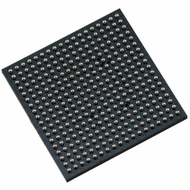
The LCMXO2280C-4FTN324I comes in a compact package that ensures easy integration into electronic circuits. The package type is FTN324.
Essence
The essence of this FPGA lies in its ability to be programmed and reprogrammed to perform specific functions, making it highly adaptable to different application requirements.
Packaging/Quantity
The LCMXO2280C-4FTN324I is typically packaged individually and is available in various quantities depending on the customer's needs.
Specifications
- Logic Elements: 2280
- Flip-Flops: 4560
- RAM Bits: 27000
- Maximum Operating Frequency: 300 MHz
- I/O Pins: 324
- Voltage Supply: 1.2V
Detailed Pin Configuration
The pin configuration of the LCMXO2280C-4FTN324I FPGA is as follows:
- Pin 1: VCCIO
- Pin 2: GND
- Pin 3: IO_0
- Pin 4: IO_1
- ...
- Pin 324: IO_323
Functional Features
- High-speed data processing capabilities
- Configurable I/O standards
- Built-in memory blocks for efficient storage and retrieval
- Support for various communication protocols
- Flexible clock management options
Advantages and Disadvantages
Advantages
- Versatile and adaptable to different applications
- Low power consumption
- Compact size allows for space-efficient designs
- High-performance capabilities
- Cost-effective compared to custom ASIC solutions
Disadvantages
- Limited resources compared to larger FPGAs
- Higher complexity in programming compared to fixed-function devices
- Not suitable for high-volume production due to higher unit costs
Working Principles
The LCMXO2280C-4FTN324I FPGA operates based on the principles of reconfigurable logic. It consists of a matrix of programmable logic elements interconnected through configurable routing channels. The device can be programmed using Hardware Description Languages (HDLs) to define the desired functionality.
Detailed Application Field Plans
The LCMXO2280C-4FTN324I FPGA finds applications in various fields, including:
- Communications: Used in wireless base stations, network routers, and data transmission systems.
- Industrial Automation: Employed in control systems, robotics, and process automation.
- Medical Devices: Integrated into medical imaging equipment, patient monitoring systems, and diagnostic instruments.
- Aerospace and Defense: Utilized in radar systems, avionics, and secure communication systems.
- Automotive: Incorporated into advanced driver-assistance systems (ADAS), infotainment systems, and engine control units (ECUs).
Detailed and Complete Alternative Models
- LCMXO2560C-4FTN324I: Similar to LCMXO2280C-4FTN324I but with increased logic elements and I/O pins.
- LCMXO640C-4FTN256I: Smaller version with reduced logic elements and I/O pins, suitable for less complex applications.
- LCMXO1200C-4FTN256I: Intermediate model with a balance of logic elements and I/O pins, suitable for medium-scale projects.
These alternative models provide options based on the specific requirements of different applications.
In conclusion, the LCMXO2280C-4FTN324I FPGA offers high-performance, low-power, and versatile programmability for various digital logic applications. Its compact size and flexible design options make it an ideal choice for a wide range of industries.
Énumérez 10 questions et réponses courantes liées à l'application de LCMXO2280C-4FTN324I dans les solutions techniques
Sure! Here are 10 common questions and answers related to the application of LCMXO2280C-4FTN324I in technical solutions:
Q: What is the LCMXO2280C-4FTN324I? A: The LCMXO2280C-4FTN324I is a low-cost, low-power FPGA (Field-Programmable Gate Array) device manufactured by Lattice Semiconductor.
Q: What are the key features of the LCMXO2280C-4FTN324I? A: Some key features include 2280 LUTs (Look-Up Tables), 80 I/O pins, 4-input look-up tables, and 324-pin FTBGA (Fine-Pitch Ball Grid Array) package.
Q: What are some typical applications of the LCMXO2280C-4FTN324I? A: The LCMXO2280C-4FTN324I can be used in various applications such as industrial control systems, automotive electronics, consumer electronics, and communication devices.
Q: How can I program the LCMXO2280C-4FTN324I? A: The LCMXO2280C-4FTN324I can be programmed using Lattice Diamond or Lattice Radiant software tools provided by Lattice Semiconductor.
Q: What voltage levels does the LCMXO2280C-4FTN324I support? A: The LCMXO2280C-4FTN324I supports both 3.3V and 1.2V voltage levels for different I/O banks.
Q: Can I use the LCMXO2280C-4FTN324I in a battery-powered device? A: Yes, the LCMXO2280C-4FTN324I is designed to be low-power and can be used in battery-powered devices.
Q: Does the LCMXO2280C-4FTN324I have any built-in communication interfaces? A: No, the LCMXO2280C-4FTN324I does not have any built-in communication interfaces. However, it can be easily interfaced with external communication modules or protocols.
Q: Can I use the LCMXO2280C-4FTN324I for real-time signal processing? A: Yes, the LCMXO2280C-4FTN324I can be used for real-time signal processing tasks by implementing appropriate algorithms and logic designs.
Q: What are the advantages of using an FPGA like LCMXO2280C-4FTN324I over a microcontroller? A: FPGAs offer higher flexibility, parallel processing capabilities, and faster execution speeds compared to microcontrollers. They are ideal for complex and computationally intensive applications.
Q: Where can I find more information about the LCMXO2280C-4FTN324I? A: You can find more detailed information, datasheets, and application notes on the official website of Lattice Semiconductor or by contacting their technical support team.