

Voir les spécifications pour les détails du produit.
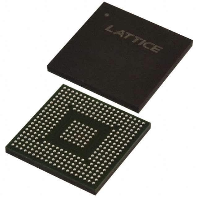
LCMXO2-4000HC-4BG332I
Product Overview
Category
The LCMXO2-4000HC-4BG332I belongs to the category of Field Programmable Gate Arrays (FPGAs).
Use
FPGAs are integrated circuits that can be programmed after manufacturing. The LCMXO2-4000HC-4BG332I is specifically designed for digital logic applications.
Characteristics
- High capacity: The LCMXO2-4000HC-4BG332I has a large number of configurable logic blocks, allowing for complex designs.
- Low power consumption: This FPGA is designed to operate efficiently with low power requirements.
- Small form factor: The compact size of the LCMXO2-4000HC-4BG332I makes it suitable for space-constrained applications.
- High-speed performance: With its optimized architecture, this FPGA offers fast processing capabilities.
Package and Quantity
The LCMXO2-4000HC-4BG332I is available in a Ball Grid Array (BGA) package. It is typically sold individually.
Specifications
- Logic Elements: 4000
- Look-Up Tables (LUTs): 3320
- Flip-Flops: 640
- Block RAM: 112 Kb
- Maximum Frequency: 150 MHz
- Operating Voltage: 1.2V
Pin Configuration
The LCMXO2-4000HC-4BG332I has a total of 332 pins. The pin configuration is as follows:
- Pin 1: VCCIO
- Pin 2: GND
- Pin 3: IO_0
- Pin 4: IO_1
- ...
- Pin 331: IO_330
- Pin 332: IO_331
Please refer to the datasheet for a complete pin configuration diagram.
Functional Features
- Configurable Logic Blocks (CLBs): The LCMXO2-4000HC-4BG332I contains multiple CLBs that can be programmed to implement various logic functions.
- I/O Interfaces: This FPGA provides numerous I/O pins for interfacing with external devices.
- Clock Management: It offers built-in clock management resources, including phase-locked loops (PLLs) and delay-locked loops (DLLs).
- Embedded Memory: The LCMXO2-4000HC-4BG332I includes on-chip memory blocks for storing data.
Advantages and Disadvantages
Advantages
- Versatility: The LCMXO2-4000HC-4BG332I can be reprogrammed, allowing for flexibility in design iterations.
- Low development cost: FPGAs eliminate the need for custom ASIC development, reducing overall costs.
- Fast time-to-market: With its programmable nature, the LCMXO2-4000HC-4BG332I enables rapid prototyping and quick product deployment.
Disadvantages
- Limited performance compared to dedicated hardware: FPGAs may not match the performance of specialized application-specific integrated circuits (ASICs) for certain applications.
- Higher power consumption: While the LCMXO2-4000HC-4BG332I is designed for low power, it still consumes more power compared to dedicated hardware solutions.
Working Principles
FPGAs like the LCMXO2-4000HC-4BG332I consist of an array of configurable logic blocks interconnected through programmable routing resources. These logic blocks can be programmed to perform specific functions using a Hardware Description Language (HDL). Upon programming, the FPGA's internal connections are established, enabling the desired functionality.
Application Field Plans
The LCMXO2-4000HC-4BG332I finds applications in various fields, including:
- Communications: It can be used for protocol conversion, signal processing, and data encryption.
- Industrial Automation: The FPGA enables control systems, motor drives, and sensor interfacing.
- Aerospace and Defense: It is suitable for radar systems, avionics, and secure communication equipment.
- Medical Devices: The LCMXO2-4000HC-4BG332I can be utilized in medical imaging, patient monitoring, and diagnostic equipment.
Alternative Models
For those seeking alternative options, the following FPGAs can be considered:
- Xilinx Spartan-6 XC6SLX9
- Altera Cyclone IV EP4CE6
- Microsemi IGLOO2 M2GL090
These alternatives offer similar capabilities and can be evaluated based on specific project requirements.
In conclusion, the LCMXO2-4000HC-4BG332I is a versatile FPGA with high capacity, low power consumption, and compact form factor. Its programmable nature allows for flexibility in design, making
Énumérez 10 questions et réponses courantes liées à l'application de LCMXO2-4000HC-4BG332I dans les solutions techniques
Sure! Here are 10 common questions and answers related to the application of LCMXO2-4000HC-4BG332I in technical solutions:
Q: What is the LCMXO2-4000HC-4BG332I? A: The LCMXO2-4000HC-4BG332I is a low-cost, low-power FPGA (Field-Programmable Gate Array) device manufactured by Lattice Semiconductor.
Q: What are the key features of LCMXO2-4000HC-4BG332I? A: Some key features include 4000 Look-Up Tables (LUTs), 332 user I/O pins, low power consumption, and support for various I/O standards.
Q: What are some typical applications of LCMXO2-4000HC-4BG332I? A: It can be used in various applications such as industrial control systems, consumer electronics, communication devices, and embedded systems.
Q: How can I program the LCMXO2-4000HC-4BG332I? A: You can program the device using Lattice Diamond or Lattice Radiant software tools provided by Lattice Semiconductor.
Q: What programming languages are supported by LCMXO2-4000HC-4BG332I? A: The device supports VHDL and Verilog hardware description languages for programming.
Q: Can I use LCMXO2-4000HC-4BG332I for high-speed data processing? A: Yes, the device supports high-speed I/O standards like LVDS, DDR, and SERDES, making it suitable for high-speed data processing applications.
Q: Does LCMXO2-4000HC-4BG332I have built-in memory? A: No, the device does not have built-in memory. However, it can interface with external memory devices through its I/O pins.
Q: What is the power consumption of LCMXO2-4000HC-4BG332I? A: The device has low power consumption, typically ranging from a few milliwatts to a few watts depending on the design and operating conditions.
Q: Can I use LCMXO2-4000HC-4BG332I in battery-powered applications? A: Yes, due to its low power consumption, the device is suitable for battery-powered applications where power efficiency is crucial.
Q: Are there any development boards available for LCMXO2-4000HC-4BG332I? A: Yes, Lattice Semiconductor provides development boards like the LCMXO2-4000HC-4BG332I-DB-EVN, which can be used for prototyping and evaluation purposes.
Please note that these answers are general and may vary based on specific requirements and use cases.