Voir les spécifications pour les détails du produit.

LC4256ZC-75TN100I
Product Overview
Category: Integrated Circuit (IC)
Use: The LC4256ZC-75TN100I is a programmable logic device (PLD) that belongs to the family of Complex Programmable Logic Devices (CPLDs). It is designed for use in various electronic applications where digital logic functions need to be implemented.
Characteristics: - High-density programmable logic device - Low power consumption - Fast performance - Flexible and reprogrammable - Small form factor - Wide operating temperature range
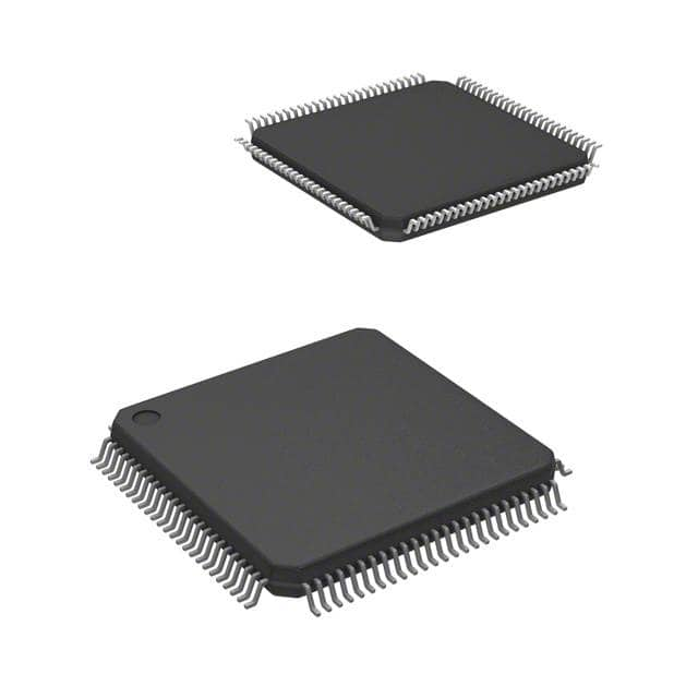
Package: The LC4256ZC-75TN100I is available in a 100-pin Thin Quad Flat Pack (TQFP) package. This package provides a compact and reliable solution for integrating the IC into electronic systems.
Essence: The essence of the LC4256ZC-75TN100I lies in its ability to implement complex digital logic functions in a single integrated circuit. It offers designers a versatile and cost-effective solution for implementing custom logic designs.
Packaging/Quantity: The LC4256ZC-75TN100I is typically sold in reels or trays, with a quantity of 250 units per reel/tray.
Specifications
- Logic Cells: 256
- Maximum User I/Os: 75
- Operating Voltage: 3.3V
- Speed Grade: Standard
- Operating Temperature Range: -40°C to 85°C
- JTAG Boundary Scan Support: Yes
- Package Type: TQFP
- Package Pins: 100
Detailed Pin Configuration
The LC4256ZC-75TN100I has a total of 100 pins, each serving a specific purpose. Here is a brief overview of the pin configuration:
- Pin 1: VCCIO - Power supply voltage for I/O banks
- Pin 2: GND - Ground reference
- Pin 3: TMS - JTAG Test Mode Select
- Pin 4: TDI - JTAG Test Data In
- Pin 5: TDO - JTAG Test Data Out
- Pin 6: TCK - JTAG Test Clock
- ...
- Pin 100: VCC - Power supply voltage
For a complete and detailed pin configuration, please refer to the LC4256ZC-75TN100I datasheet.
Functional Features
The LC4256ZC-75TN100I offers several functional features that make it suitable for a wide range of applications:
- Programmability: The device can be programmed to implement various digital logic functions, allowing designers to create custom solutions.
- High-Density Logic Cells: With 256 logic cells, the IC can handle complex logic designs efficiently.
- Low Power Consumption: The device is designed to operate with low power consumption, making it suitable for battery-powered applications.
- Fast Performance: The IC offers fast propagation delays, enabling high-speed operation in time-critical applications.
- Flexible I/O Configuration: The device supports up to 75 user I/Os, providing flexibility in interfacing with other components.
- JTAG Boundary Scan Support: The built-in JTAG boundary scan support allows for easy testing and debugging of the device during development.
Advantages and Disadvantages
Advantages: - Versatile and flexible programmability - High-density logic cells for complex designs - Low power consumption - Fast performance - Wide operating temperature range
Disadvantages: - Limited number of user I/Os compared to some other devices - Relatively small package size may limit the number of available pins for larger designs
Working Principles
The LC4256ZC-75TN100I operates based on the principles of programmable logic. It consists of an array of configurable logic blocks (CLBs) interconnected through a programmable routing matrix. The CLBs can be configured to implement various logic functions, such as AND, OR, XOR, and more. The interconnections between the CLBs are established using programmable switches, allowing designers to create custom logic designs.
During operation, the device reads the configuration data from an external memory source and configures its internal logic accordingly. This allows for the implementation of complex digital logic functions within a single IC.
Detailed Application Field Plans
The LC4256ZC-75TN100I finds applications in various fields, including:
- Embedded Systems: The device can be used in embedded systems to implement custom logic functions, such as control and interface modules.
- Communications: It can be utilized in communication systems for protocol handling, signal processing, and data manipulation.
- Industrial Automation: The IC can be employed in industrial automation systems for controlling and monitoring processes.
- Consumer Electronics: It finds use in consumer electronics products,
Énumérez 10 questions et réponses courantes liées à l'application de LC4256ZC-75TN100I dans les solutions techniques
Sure! Here are 10 common questions and answers related to the application of LC4256ZC-75TN100I in technical solutions:
Q: What is LC4256ZC-75TN100I? A: LC4256ZC-75TN100I is a specific model of a low-cost, low-power FPGA (Field-Programmable Gate Array) manufactured by Lattice Semiconductor.
Q: What are the key features of LC4256ZC-75TN100I? A: Some key features of LC4256ZC-75TN100I include 256 macrocells, 75MHz maximum operating frequency, 100-pin TQFP package, and low power consumption.
Q: What are the typical applications of LC4256ZC-75TN100I? A: LC4256ZC-75TN100I is commonly used in various technical solutions such as industrial automation, consumer electronics, telecommunications, automotive systems, and more.
Q: How can I program LC4256ZC-75TN100I? A: LC4256ZC-75TN100I can be programmed using Lattice Diamond or iCEcube2 software tools provided by Lattice Semiconductor.
Q: What programming languages are supported by LC4256ZC-75TN100I? A: LC4256ZC-75TN100I supports popular hardware description languages (HDLs) like VHDL and Verilog for programming.
Q: Can LC4256ZC-75TN100I be reprogrammed after initial programming? A: Yes, LC4256ZC-75TN100I is a reprogrammable FPGA, allowing you to modify and reconfigure its functionality as needed.
Q: What is the power supply requirement for LC4256ZC-75TN100I? A: LC4256ZC-75TN100I typically operates on a 3.3V power supply, but it also supports a wide voltage range from 2.25V to 3.6V.
Q: Can LC4256ZC-75TN100I interface with other components or devices? A: Yes, LC4256ZC-75TN100I can interface with various components and devices through its I/O pins, supporting protocols like SPI, I2C, UART, etc.
Q: Are there any development boards available for LC4256ZC-75TN100I? A: Yes, Lattice Semiconductor offers development boards specifically designed for LC4256ZC-75TN100I, which provide a convenient platform for prototyping and testing.
Q: Where can I find more technical documentation and support for LC4256ZC-75TN100I? A: You can find detailed technical documentation, datasheets, application notes, and support resources on the official website of Lattice Semiconductor or by contacting their customer support team.

