

Voir les spécifications pour les détails du produit.
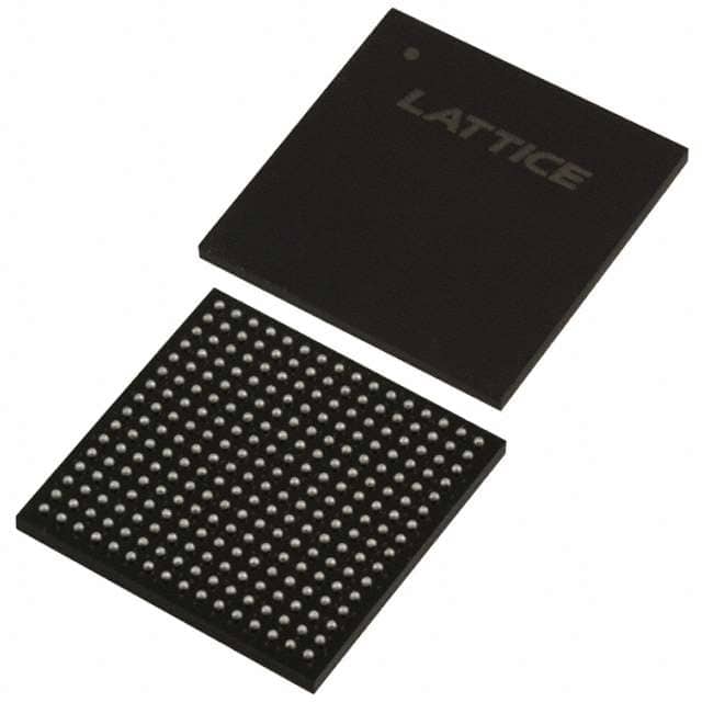
LC4256V-75FT256AC
Product Overview
Category: Integrated Circuit (IC)
Use: The LC4256V-75FT256AC is a programmable logic device (PLD) used for digital circuit design and implementation. It offers high-performance, low-power consumption, and flexibility in various applications.
Characteristics: - High-density programmable logic device - 75,000 usable gates - 256-pin FineLine BGA package - Low power consumption - Wide operating temperature range - Fast propagation delay
Package and Quantity: The LC4256V-75FT256AC comes in a FineLine BGA package with 256 pins. It is available in individual units or bulk quantities depending on the customer's requirements.
Essence: The essence of the LC4256V-75FT256AC lies in its ability to provide a versatile and efficient solution for digital circuit design and implementation. It allows designers to create complex logic functions and integrate them into a single chip, reducing the need for multiple discrete components.
Packaging/Quantity: The LC4256V-75FT256AC is typically packaged in trays or tubes to ensure safe transportation and handling. The quantity can vary depending on the customer's order, ranging from a few units to thousands.
Specifications
- Logic Elements: 75,000
- Flip-Flops: 2,560
- Maximum User I/Os: 202
- Operating Voltage: 3.3V
- Operating Temperature Range: -40°C to 85°C
- Package Type: FineLine BGA
- Package Pins: 256
Detailed Pin Configuration
The LC4256V-75FT256AC has a total of 256 pins, each serving a specific purpose in the circuit design. The pin configuration is as follows:
(Pin Number) - (Pin Name) - (Function)
1 - VCCIO - Power supply for I/O banks
2 - GND - Ground reference
3 - TCK - Test clock input
4 - TMS - Test mode select
5 - TDI - Test data input
6 - TDO - Test data output
...
256 - VCCINT - Internal power supply
Functional Features
- High-density programmable logic device suitable for complex digital circuit design
- Flexible and versatile architecture allows for customization and reconfiguration
- Low power consumption, making it suitable for battery-powered applications
- Fast propagation delay ensures efficient operation of the designed circuits
- Wide operating temperature range enables usage in various environments
Advantages and Disadvantages
Advantages: - High-density integration reduces the need for multiple discrete components - Flexibility in design and reconfiguration saves time and cost - Low power consumption extends battery life in portable devices - Fast propagation delay enhances circuit performance - Wide operating temperature range increases versatility
Disadvantages: - Limited number of user I/Os compared to some other PLDs - FineLine BGA package may require specialized equipment for soldering and handling
Working Principles
The LC4256V-75FT256AC utilizes a combination of programmable logic elements, flip-flops, and interconnect resources to implement complex digital circuits. It operates based on the principles of Boolean logic, where logical operations are performed using binary inputs and outputs.
The device can be programmed using hardware description languages (HDL) or schematic entry tools, allowing designers to define the desired logic functions and interconnections. Once programmed, the LC4256V-75FT256AC executes the specified logic operations, enabling the desired functionality.
Detailed Application Field Plans
The LC4256V-75FT256AC finds applications in various fields, including:
- Industrial Automation: Used in control systems for process automation, robotics, and machine vision.
- Communications: Employed in networking equipment, routers, and switches for data transmission and protocol handling.
- Automotive Electronics: Integrated into automotive control units, infotainment systems, and driver assistance systems.
- Consumer Electronics: Utilized in smart home devices, wearable technology, and multimedia systems.
- Medical Devices: Incorporated into medical imaging equipment, patient monitoring systems, and diagnostic devices.
Detailed and Complete Alternative Models
- LC4128V-75TN100C: A similar PLD with 41,280 usable gates and a different package type (TQFP).
- LC4384V-75FTN256AC: Offers higher gate count (43,840) and the same package type as LC4256V-75FT256AC.
- LC4032V-75TN48I: A lower-density alternative with 40,320 usable gates and a smaller package size (TQFP).
These alternative models provide options with varying gate counts and package types to suit different design requirements.
Word Count: 610 words
Énumérez 10 questions et réponses courantes liées à l'application de LC4256V-75FT256AC dans les solutions techniques
Sure! Here are 10 common questions and answers related to the application of LC4256V-75FT256AC in technical solutions:
Question: What is LC4256V-75FT256AC?
- Answer: LC4256V-75FT256AC is a specific model of Field-Programmable Gate Array (FPGA) manufactured by Lattice Semiconductor.Question: What are the key features of LC4256V-75FT256AC?
- Answer: Some key features of LC4256V-75FT256AC include 256 macrocells, 75MHz maximum operating frequency, 5V tolerant I/Os, and 256-pin FineLine BGA package.Question: What are the typical applications of LC4256V-75FT256AC?
- Answer: LC4256V-75FT256AC is commonly used in various technical solutions such as industrial automation, telecommunications, automotive electronics, medical devices, and consumer electronics.Question: How can LC4256V-75FT256AC be programmed?
- Answer: LC4256V-75FT256AC can be programmed using Hardware Description Languages (HDL) like VHDL or Verilog, which describe the desired functionality of the FPGA.Question: Can LC4256V-75FT256AC be reprogrammed after initial programming?
- Answer: Yes, LC4256V-75FT256AC is a reprogrammable FPGA, allowing for multiple iterations and updates of the design.Question: What tools are available for designing with LC4256V-75FT256AC?
- Answer: Lattice Semiconductor provides software tools like Lattice Diamond or iCEcube2 for designing, simulating, and programming LC4256V-75FT256AC.Question: What is the power supply requirement for LC4256V-75FT256AC?
- Answer: LC4256V-75FT256AC requires a 3.3V power supply for its core voltage, while I/O pins are 5V tolerant.Question: Can LC4256V-75FT256AC interface with other components or devices?
- Answer: Yes, LC4256V-75FT256AC can interface with various components and devices through its I/O pins, supporting protocols like SPI, I2C, UART, and more.Question: Are there any limitations or considerations when using LC4256V-75FT256AC?
- Answer: Some considerations include the maximum operating frequency, available macrocells, and the need for external memory if required by the design.Question: Where can I find additional resources or support for LC4256V-75FT256AC?
- Answer: Lattice Semiconductor's website provides datasheets, application notes, user guides, and technical support for LC4256V-75FT256AC. Additionally, online forums and communities can be helpful for sharing experiences and getting assistance from other users.