

Voir les spécifications pour les détails du produit.
LC4064ZC-75M132C
Product Overview
Category: Integrated Circuit (IC)
Use: The LC4064ZC-75M132C is a programmable logic device (PLD) that belongs to the family of Complex Programmable Logic Devices (CPLDs). It is designed for digital logic applications and offers high-performance, low-power consumption, and flexibility in circuit design.
Characteristics: - High-density integration - Low power consumption - Flexible programming options - Fast propagation delay - Wide operating temperature range
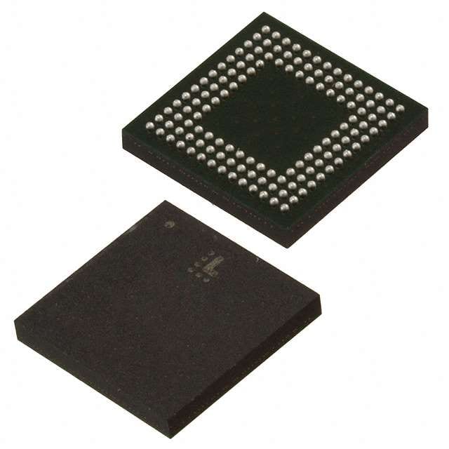
Package: The LC4064ZC-75M132C is available in a compact 132-pin plastic quad flat pack (PQFP) package. This package provides excellent thermal performance and ease of handling during assembly.
Essence: The essence of the LC4064ZC-75M132C lies in its ability to implement complex digital logic functions in a single integrated circuit. It offers designers the flexibility to create custom logic circuits tailored to their specific application requirements.
Packaging/Quantity: The LC4064ZC-75M132C is typically sold in reels or trays, with each reel or tray containing a specified quantity of ICs. The exact packaging and quantity may vary depending on the supplier.
Specifications
- Maximum Operating Frequency: 75 MHz
- Number of Logic Cells: 4,064
- Number of I/O Pins: 132
- Supply Voltage: 3.3V
- Operating Temperature Range: -40°C to +85°C
- Programming Technology: In-system programmable (ISP)
- Package Dimensions: 20mm x 20mm
Detailed Pin Configuration
The LC4064ZC-75M132C has a total of 132 pins, which are assigned to various functions such as input, output, clock, and power supply. The detailed pin configuration can be found in the product datasheet provided by the manufacturer.
Functional Features
- Programmable Logic: The LC4064ZC-75M132C offers a large number of programmable logic cells that can be configured to implement various digital logic functions.
- I/O Flexibility: It provides a sufficient number of I/O pins for interfacing with external devices, allowing for versatile connectivity options.
- Clock Management: The device supports multiple clock inputs and provides advanced clock management features such as clock division and multiplication.
- Embedded Memory: The LC4064ZC-75M132C includes embedded memory blocks that can be used for storing data or implementing lookup tables.
- JTAG Interface: It features a JTAG (Joint Test Action Group) interface for easy programming and debugging.
Advantages and Disadvantages
Advantages: - High integration density allows for complex circuit implementation in a single device. - Low power consumption makes it suitable for battery-powered applications. - Flexible programming options enable customization and iterative design. - Fast propagation delay ensures efficient signal processing. - Wide operating temperature range enables usage in various environments.
Disadvantages: - Limited number of logic cells compared to larger CPLDs or FPGAs. - Relatively small package size may restrict the number of I/O pins available for certain applications. - Programming complexity may require specialized knowledge or tools.
Working Principles
The LC4064ZC-75M132C operates based on the principles of programmable logic. It consists of an array of configurable logic cells interconnected through programmable routing resources. These logic cells can be programmed to implement desired logic functions using hardware description languages or dedicated software tools. The resulting configuration is stored in non-volatile memory within the device and remains intact even after power is removed.
During operation, the input signals are processed through the configured logic cells, and the output signals are generated accordingly. The device can be reprogrammed multiple times to modify the logic functions or adapt to changing requirements.
Detailed Application Field Plans
The LC4064ZC-75M132C finds applications in various fields, including but not limited to: 1. Industrial Automation: It can be used for control and monitoring systems in manufacturing processes. 2. Communication Systems: It enables the implementation of digital signal processing algorithms and protocol handling. 3. Consumer Electronics: It can be utilized in audio/video processing, gaming consoles, and home automation systems. 4. Automotive Electronics: It finds applications in vehicle control units, driver assistance systems, and infotainment systems. 5. Medical Devices: It can be employed in medical imaging equipment, patient monitoring systems, and laboratory instruments.
Detailed and Complete Alternative Models
- LC4032ZC-75M132C: Similar to LC4064ZC-75M132C but with a lower number of logic cells (4,032).
- LC4128ZC-75M132C: Similar to LC4064ZC-75M132C but with a higher number of
Énumérez 10 questions et réponses courantes liées à l'application de LC4064ZC-75M132C dans les solutions techniques
Sure! Here are 10 common questions and answers related to the application of LC4064ZC-75M132C in technical solutions:
Q: What is LC4064ZC-75M132C? A: LC4064ZC-75M132C is a specific model of field-programmable gate array (FPGA) manufactured by Lattice Semiconductor.
Q: What are the key features of LC4064ZC-75M132C? A: LC4064ZC-75M132C offers 64 macrocells, 64 I/O pins, 75MHz maximum operating frequency, and 132-pin package.
Q: What are the typical applications of LC4064ZC-75M132C? A: LC4064ZC-75M132C is commonly used in various technical solutions such as industrial automation, telecommunications, automotive electronics, and consumer electronics.
Q: How can LC4064ZC-75M132C be programmed? A: LC4064ZC-75M132C can be programmed using hardware description languages (HDLs) like VHDL or Verilog, or through graphical programming tools provided by Lattice Semiconductor.
Q: Can LC4064ZC-75M132C be reprogrammed after initial programming? A: Yes, LC4064ZC-75M132C is a reprogrammable FPGA, allowing for multiple programming cycles.
Q: What voltage levels does LC4064ZC-75M132C support? A: LC4064ZC-75M132C supports both 3.3V and 5V voltage levels, making it compatible with a wide range of systems.
Q: Does LC4064ZC-75M132C have built-in memory? A: No, LC4064ZC-75M132C does not have built-in memory. However, it can interface with external memory devices.
Q: Can LC4064ZC-75M132C communicate with other components or devices? A: Yes, LC4064ZC-75M132C supports various communication protocols such as SPI, I2C, UART, and CAN, enabling seamless integration with other components or devices.
Q: What development tools are available for programming LC4064ZC-75M132C? A: Lattice Semiconductor provides software tools like Lattice Diamond and iCEcube2 for designing, simulating, and programming LC4064ZC-75M132C.
Q: Are there any application-specific reference designs available for LC4064ZC-75M132C? A: Yes, Lattice Semiconductor offers reference designs and application notes that provide guidance on implementing specific functionalities using LC4064ZC-75M132C in different applications.
Please note that the answers provided here are general and may vary depending on the specific requirements and use cases of LC4064ZC-75M132C in technical solutions.