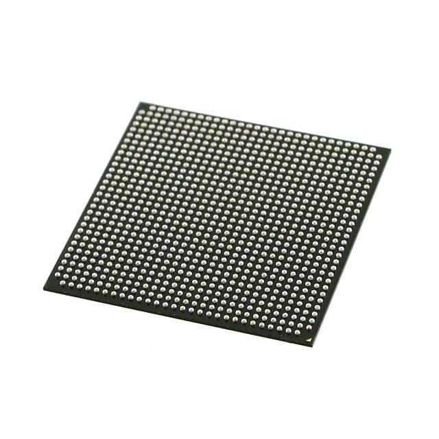
Voir les spécifications pour les détails du produit.

EP2C70F896C8N
Basic Information Overview
- Category: Integrated Circuit (IC)
- Use: Field Programmable Gate Array (FPGA)
- Characteristics: High-performance, low-power consumption, reconfigurable logic device
- Package: 896-pin FineLine BGA package
- Essence: FPGA with advanced features and capabilities
- Packaging/Quantity: Single unit per package
Specifications
- Manufacturer: Intel Corporation
- Family: Cyclone II
- Device Type: FPGA
- Logic Elements: 70,208
- RAM Bits: 3,888 Kbits
- Embedded Multipliers: 288
- Maximum Operating Frequency: 400 MHz
- Voltage Supply: 1.2V
- Temperature Range: -40°C to +100°C
Detailed Pin Configuration
The EP2C70F896C8N has a total of 896 pins arranged in a FineLine BGA package. The pin configuration includes various types of pins such as power supply pins, ground pins, I/O pins, clock pins, configuration pins, and programming pins. Each pin serves a specific purpose and is labeled accordingly.
Functional Features
- High-performance FPGA with advanced architecture
- Reconfigurable logic elements for flexible design implementation
- Embedded multipliers for efficient multiplication operations
- Dedicated memory blocks for data storage
- Support for various communication protocols and interfaces
- On-chip PLLs for clock generation and synchronization
- Built-in configuration circuitry for easy programming
Advantages and Disadvantages
Advantages: - High-performance computing capabilities - Flexibility and reconfigurability for rapid prototyping - Low-power consumption compared to traditional ASICs - Support for various communication standards - Large number of logic elements and memory blocks
Disadvantages: - Higher cost compared to general-purpose microcontrollers - Steeper learning curve for FPGA programming - Limited availability of alternative models with similar specifications
Working Principles
The EP2C70F896C8N is based on the Field Programmable Gate Array (FPGA) technology. It consists of a large number of configurable logic elements, memory blocks, and embedded multipliers. These components can be programmed to implement desired digital circuits and functions. The FPGA can be reconfigured multiple times, allowing for flexibility in design and prototyping. The device operates by receiving input signals, processing them through the configured logic elements, and producing the desired output signals.
Detailed Application Field Plans
The EP2C70F896C8N FPGA finds applications in various fields, including: 1. Telecommunications: Used in base stations, network routers, and communication equipment for signal processing and protocol handling. 2. Industrial Automation: Employed in control systems, robotics, and machine vision applications for real-time data processing and control. 3. Automotive: Utilized in advanced driver-assistance systems (ADAS), engine control units (ECUs), and infotainment systems for high-performance computing tasks. 4. Aerospace and Defense: Integrated into radar systems, avionics, and military-grade equipment for signal processing, encryption, and communication. 5. Medical Devices: Applied in medical imaging, patient monitoring, and diagnostic equipment for data processing and analysis.
Detailed and Complete Alternative Models
- EP2C35F672C6N: A smaller variant with 35,648 logic elements and 672-pin package.
- EP2C70F672C6N: Similar to EP2C70F896C8N but with a 672-pin package.
- EP2C70Q240C8N: Offers 70,208 logic elements in a quad flat pack (QFP) package with 240 pins.
- EP2C70F484C7N: Features 70,208 logic elements in a 484-pin FineLine BGA package.
These alternative models provide different pin configurations and package options while maintaining similar logic element counts and functionality.
Word count: 369 words
Énumérez 10 questions et réponses courantes liées à l'application de EP2C70F896C8N dans les solutions techniques
Sure! Here are 10 common questions and answers related to the application of EP2C70F896C8N in technical solutions:
Q: What is EP2C70F896C8N? A: EP2C70F896C8N is a field-programmable gate array (FPGA) chip manufactured by Intel.
Q: What are the key features of EP2C70F896C8N? A: Some key features include 70,000 logic elements, 896 user I/O pins, and support for various communication protocols.
Q: What are the typical applications of EP2C70F896C8N? A: EP2C70F896C8N is commonly used in applications such as digital signal processing, image and video processing, and high-performance computing.
Q: Can EP2C70F896C8N be used in industrial automation systems? A: Yes, EP2C70F896C8N can be used in industrial automation systems for tasks like control and monitoring.
Q: Does EP2C70F896C8N support Ethernet connectivity? A: Yes, EP2C70F896C8N supports Ethernet connectivity through dedicated MAC (Media Access Control) IP cores.
Q: Can EP2C70F896C8N interface with external memory devices? A: Yes, EP2C70F896C8N has built-in memory controllers that allow it to interface with external memory devices like DDR SDRAM.
Q: Is EP2C70F896C8N suitable for real-time applications? A: Yes, EP2C70F896C8N can be used in real-time applications due to its high-speed processing capabilities and low-latency I/O.
Q: Can EP2C70F896C8N be reprogrammed after deployment? A: Yes, EP2C70F896C8N is a field-programmable device, meaning it can be reprogrammed even after it has been deployed in a system.
Q: What development tools are available for programming EP2C70F896C8N? A: Intel provides Quartus Prime software, which includes a suite of tools for designing, simulating, and programming EP2C70F896C8N.
Q: Are there any limitations or considerations when using EP2C70F896C8N? A: Some considerations include power consumption, heat dissipation, and the need for proper signal integrity design to ensure reliable operation.
Please note that these answers are general and may vary depending on specific requirements and implementation details.

