

Voir les spécifications pour les détails du produit.
5SGXEABK2H40C2LN
Basic Information Overview
- Category: Field Programmable Gate Array (FPGA)
- Use: Digital logic circuits and systems design
- Characteristics: High-performance, reconfigurable, programmable
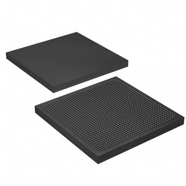
- Package: BGA (Ball Grid Array)
- Essence: Integrated circuit for customizable digital logic implementation
- Packaging/Quantity: Single unit
Specifications
- Manufacturer: Intel Corporation
- Series: Stratix V
- Model: 5SGXEABK2H40C2LN
- Logic Elements: 462,000
- Embedded Memory: 25,920 Kbits
- DSP Blocks: 3,888
- Maximum User I/Os: 1,280
- Operating Voltage: 1.0V
- Speed Grade: -2
- Package Type: 1517-Ball Flip-Chip BGA
Detailed Pin Configuration
The detailed pin configuration of 5SGXEABK2H40C2LN can be found in the manufacturer's datasheet.
Functional Features
- High-speed performance with advanced architecture
- Reconfigurable logic elements for flexible design
- Embedded memory blocks for efficient data storage
- Dedicated DSP blocks for signal processing tasks
- Support for various communication protocols
- On-chip clock management resources
- Built-in security features for IP protection
Advantages
- Versatile and customizable for a wide range of applications
- High-performance computing capabilities
- Lower power consumption compared to traditional ASIC designs
- Faster time-to-market due to reprogrammability
- Cost-effective solution for prototyping and low-volume production
Disadvantages
- Higher cost compared to general-purpose microcontrollers
- Limited scalability for large-scale designs
- Steeper learning curve for FPGA programming
- More complex debugging and verification process
Working Principles
5SGXEABK2H40C2LN is based on the principle of field programmability, where the logic elements and interconnects can be configured to implement desired digital circuits. The device consists of configurable logic blocks (CLBs), memory blocks, DSP blocks, I/O interfaces, and other supporting resources. The user designs the desired circuit using a hardware description language (HDL) and programs it onto the FPGA using specialized software tools. Once programmed, the FPGA executes the designed circuit by routing signals through the configured logic elements.
Detailed Application Field Plans
- Digital signal processing
- High-speed data communication
- Image and video processing
- Cryptography and security systems
- Industrial automation and control
- Aerospace and defense systems
- Scientific research and prototyping
Detailed and Complete Alternative Models
- 5SGXEA7N2F45C2LN
- 5SGXEB6R3F43C2LN
- 5SGXEB9R3F43C2LN
- 5SGXEBBR3F43C2LN
- 5SGXEBDR3F43C2LN
(Note: This list is not exhaustive and alternative models may vary based on specific requirements.)
This entry provides an overview of the 5SGXEABK2H40C2LN FPGA, including its basic information, specifications, pin configuration, functional features, advantages, disadvantages, working principles, application field plans, and alternative models. It serves as a comprehensive reference for understanding and utilizing this particular FPGA model in various digital logic design applications.
Énumérez 10 questions et réponses courantes liées à l'application de 5SGXEABK2H40C2LN dans les solutions techniques
Sure! Here are 10 common questions and answers related to the application of 5SGXEABK2H40C2LN in technical solutions:
Q: What is the purpose of the 5SGXEABK2H40C2LN FPGA? A: The 5SGXEABK2H40C2LN is a Field-Programmable Gate Array (FPGA) designed for implementing complex digital logic circuits in various technical solutions.
Q: What are some typical applications of the 5SGXEABK2H40C2LN FPGA? A: This FPGA can be used in applications such as high-performance computing, telecommunications, industrial automation, image processing, and data center acceleration.
Q: How does the 5SGXEABK2H40C2LN FPGA differ from other FPGAs? A: The 5SGXEABK2H40C2LN offers a unique combination of high-speed transceivers, large capacity, and low power consumption, making it suitable for demanding applications.
Q: Can I program the 5SGXEABK2H40C2LN FPGA using industry-standard tools? A: Yes, this FPGA can be programmed using popular design software like Intel Quartus Prime, which provides a comprehensive development environment.
Q: What is the maximum number of logic elements available in the 5SGXEABK2H40C2LN FPGA? A: The 5SGXEABK2H40C2LN has a maximum of 40,000 logic elements, allowing for the implementation of complex designs.
Q: Does the 5SGXEABK2H40C2LN support high-speed serial communication? A: Yes, this FPGA includes high-speed transceivers that support protocols like PCIe, Ethernet, USB, and SATA, enabling fast data transfer.
Q: Can I use the 5SGXEABK2H40C2LN in safety-critical applications? A: Yes, this FPGA offers features like error correction codes (ECC) and built-in self-test (BIST), making it suitable for safety-critical systems.
Q: What is the power consumption of the 5SGXEABK2H40C2LN FPGA? A: The power consumption varies depending on the design and operating conditions, but generally, this FPGA has low power consumption compared to alternatives.
Q: Does the 5SGXEABK2H40C2LN support partial reconfiguration? A: Yes, this FPGA supports partial reconfiguration, allowing specific sections of the design to be updated without affecting the entire system.
Q: Are there any development boards available for prototyping with the 5SGXEABK2H40C2LN FPGA? A: Yes, Intel provides development kits and evaluation boards specifically designed for the 5SGXEABK2H40C2LN FPGA, which can be used for prototyping and testing.
Please note that the specific details and answers may vary based on the manufacturer's documentation and the application requirements.