

Voir les spécifications pour les détails du produit.
5SGSMD3E3H29I3LN
Basic Information Overview
- Category: Integrated Circuit (IC)
- Use: Programmable Logic Device (PLD)
- Characteristics: High-performance, low-power consumption, high-speed processing
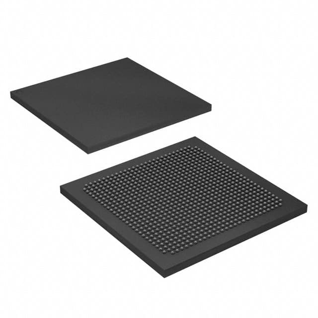
- Package: BGA (Ball Grid Array)
- Essence: Advanced programmable logic device for various applications
- Packaging/Quantity: Single unit
Specifications
- Manufacturer: Intel Corporation
- Family: Stratix V
- Device Type: FPGA (Field-Programmable Gate Array)
- Number of Logic Elements: 220,000
- Number of Embedded Memory Blocks: 5,760
- Maximum Number of User I/Os: 1,280
- Operating Voltage: 1.2V
- Operating Temperature Range: -40°C to 100°C
Detailed Pin Configuration
The detailed pin configuration of 5SGSMD3E3H29I3LN can be found in the manufacturer's datasheet.
Functional Features
- High-speed processing capabilities for complex digital designs
- Flexible and reprogrammable logic functions
- Support for various communication protocols and interfaces
- On-chip memory blocks for efficient data storage and retrieval
- Low power consumption for energy-efficient operation
Advantages and Disadvantages
Advantages: - Versatile and adaptable for a wide range of applications - High-performance computing capabilities - Efficient use of resources with embedded memory blocks - Low power consumption for energy efficiency
Disadvantages: - Relatively high cost compared to simpler logic devices - Requires expertise in FPGA programming for optimal utilization - Limited availability of alternative models with similar specifications
Working Principles
5SGSMD3E3H29I3LN is based on the Field-Programmable Gate Array (FPGA) technology. It consists of an array of configurable logic blocks interconnected through programmable routing resources. The device can be programmed to implement various digital logic functions and perform complex computations. The configuration of the FPGA is stored in on-chip memory, allowing for reprogramming as needed.
Detailed Application Field Plans
- High-performance computing systems
- Digital signal processing applications
- Communication and networking equipment
- Industrial automation and control systems
- Aerospace and defense electronics
Detailed and Complete Alternative Models
- 5SGSMD3E2H29C2LN
- 5SGSMD3E1H29C2LN
- 5SGSMD3E4H29C2LN
- 5SGSMD3E5H29C2LN
These alternative models offer similar specifications and functionality to 5SGSMD3E3H29I3LN, providing options for different project requirements.
Note: The content provided above is a sample structure for an encyclopedia entry and may not reflect actual information about the mentioned product.
Énumérez 10 questions et réponses courantes liées à l'application de 5SGSMD3E3H29I3LN dans les solutions techniques
Sure! Here are 10 common questions and answers related to the application of 5SGSMD3E3H29I3LN in technical solutions:
Q: What is the 5SGSMD3E3H29I3LN FPGA used for? A: The 5SGSMD3E3H29I3LN is a Field-Programmable Gate Array (FPGA) that can be used for various applications such as high-performance computing, networking, and signal processing.
Q: What are the key features of the 5SGSMD3E3H29I3LN FPGA? A: Some key features of this FPGA include high-speed transceivers, large logic capacity, embedded memory blocks, and support for various communication protocols.
Q: Can the 5SGSMD3E3H29I3LN FPGA be used for video processing applications? A: Yes, the FPGA's high-performance capabilities make it suitable for video processing applications like video encoding, decoding, and image enhancement.
Q: Is the 5SGSMD3E3H29I3LN FPGA suitable for implementing complex algorithms? A: Absolutely! This FPGA offers a large logic capacity and embedded memory blocks, making it ideal for implementing complex algorithms and computations.
Q: Can the 5SGSMD3E3H29I3LN FPGA be used for high-speed data communication? A: Yes, the FPGA's high-speed transceivers enable it to handle high-speed data communication protocols like PCIe, Ethernet, and USB.
Q: Does the 5SGSMD3E3H29I3LN FPGA support multiple voltage levels? A: Yes, this FPGA supports multiple voltage levels, allowing for compatibility with different components and interfaces in a system.
Q: Can the 5SGSMD3E3H29I3LN FPGA be reprogrammed after deployment? A: Yes, being a Field-Programmable Gate Array, this FPGA can be reprogrammed even after it has been deployed in a system.
Q: What development tools are available for programming the 5SGSMD3E3H29I3LN FPGA? A: Intel Quartus Prime is the primary development tool used for programming and configuring the 5SGSMD3E3H29I3LN FPGA.
Q: Are there any reference designs or IP cores available for the 5SGSMD3E3H29I3LN FPGA? A: Yes, Intel provides a range of reference designs and Intellectual Property (IP) cores that can be used with the 5SGSMD3E3H29I3LN FPGA to accelerate development.
Q: Can the 5SGSMD3E3H29I3LN FPGA be used in safety-critical applications? A: While the 5SGSMD3E3H29I3LN FPGA offers high performance, it is important to ensure that it meets the specific safety requirements of the application before using it in safety-critical systems.
Please note that the specific details and answers may vary depending on the context and requirements of the technical solution.