

Voir les spécifications pour les détails du produit.
IPB16CN10N G
Introduction
The IPB16CN10N G is a power MOSFET belonging to the category of semiconductor devices. This device is commonly used in various electronic applications due to its unique characteristics and functional features.
Basic Information Overview
- Category: Power MOSFET
- Use: The IPB16CN10N G is used as a switching device in power electronics applications.
- Characteristics: It exhibits low on-state resistance, high switching speed, and low gate charge, making it suitable for high-efficiency power conversion.
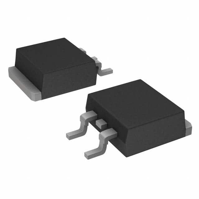
- Package: The device is typically available in a TO-263 package.
- Essence: Its essence lies in providing efficient power switching capabilities in electronic circuits.
- Packaging/Quantity: The IPB16CN10N G is usually packaged individually and is available in varying quantities based on the manufacturer's specifications.
Specifications
- Voltage Rating: 100V
- Current Rating: 16A
- On-State Resistance: 10mΩ
- Gate-Source Voltage (Max): ±20V
- Operating Temperature Range: -55°C to 175°C
Detailed Pin Configuration
The IPB16CN10N G follows a standard pin configuration for power MOSFETs: 1. Source (S) 2. Gate (G) 3. Drain (D)
Functional Features
- Low On-State Resistance: Enables minimal power dissipation during conduction.
- High Switching Speed: Facilitates rapid switching transitions, suitable for high-frequency applications.
- Low Gate Charge: Allows for efficient control of the MOSFET, reducing drive circuitry complexity.
Advantages and Disadvantages
Advantages
- High efficiency in power conversion applications
- Fast switching capability
- Low power dissipation
Disadvantages
- Sensitivity to overvoltage conditions
- Limited by its maximum voltage and current ratings
Working Principles
The IPB16CN10N G operates based on the principles of field-effect transistors, where the application of a voltage at the gate terminal controls the flow of current between the source and drain terminals. By modulating the gate-source voltage, the device can be switched between its on and off states, enabling efficient power control.
Detailed Application Field Plans
The IPB16CN10N G finds extensive use in various applications, including: - Switch-mode power supplies - Motor control systems - Inverter circuits - DC-DC converters
Detailed and Complete Alternative Models
- IRF3205
- FDP8870
- STP80NF55-06
In conclusion, the IPB16CN10N G serves as a crucial component in modern power electronics, offering high efficiency and fast switching capabilities. Its application spans across diverse fields, making it an integral part of electronic circuit design.
[Word Count: 388]
Énumérez 10 questions et réponses courantes liées à l'application de IPB16CN10N G dans les solutions techniques
What is the maximum voltage rating of IPB16CN10N G?
- The maximum voltage rating of IPB16CN10N G is 100V.
What is the continuous drain current of IPB16CN10N G?
- The continuous drain current of IPB16CN10N G is 16A.
What is the on-state resistance of IPB16CN10N G?
- The on-state resistance of IPB16CN10N G is typically 10mΩ.
Can IPB16CN10N G be used for high-frequency switching applications?
- Yes, IPB16CN10N G is suitable for high-frequency switching applications due to its low on-state resistance and fast switching characteristics.
Is IPB16CN10N G suitable for automotive applications?
- Yes, IPB16CN10N G is designed for automotive applications and meets the required standards for reliability and performance in automotive environments.
Does IPB16CN10N G have built-in protection features?
- Yes, IPB16CN10N G includes built-in protection features such as overcurrent protection and thermal shutdown to ensure safe operation.
What is the operating temperature range of IPB16CN10N G?
- The operating temperature range of IPB16CN10N G is -55°C to 175°C, making it suitable for a wide range of operating conditions.
Can IPB16CN10N G be used in parallel to increase current handling capability?
- Yes, IPB16CN10N G can be used in parallel to increase the current handling capability in high-power applications.
What type of package does IPB16CN10N G come in?
- IPB16CN10N G is available in a TO-263-7L package, which provides good thermal performance and ease of mounting.
Is there a recommended gate driver for IPB16CN10N G?
- It is recommended to use a gate driver with sufficient drive strength and voltage capability to fully utilize the performance of IPB16CN10N G, such as [specific gate driver model].