

Voir les spécifications pour les détails du produit.
QS3L384PAG8
Product Overview
- Category: Integrated Circuit (IC)
- Use: Digital Multiplexer/Demultiplexer
- Characteristics: High-speed, low-power, compact design
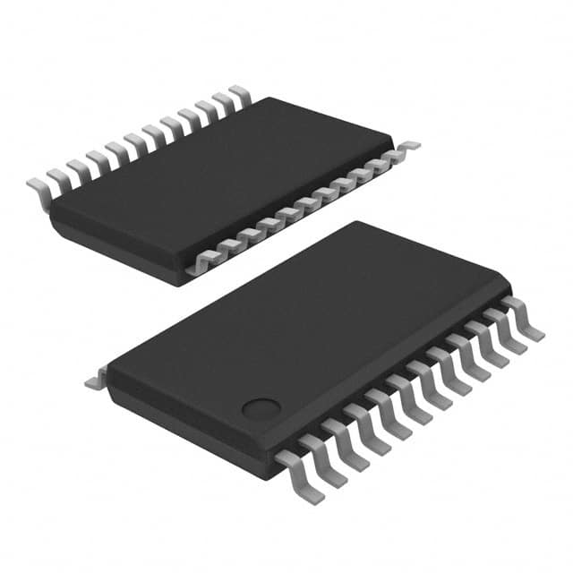
- Package: 48-pin Thin Quad Flat Pack (TQFP)
- Essence: Efficient data routing and selection
- Packaging/Quantity: Available in reels of 250 units
Specifications
- Technology: CMOS
- Supply Voltage: 2.5V - 3.3V
- Operating Temperature: -40°C to +85°C
- Input/Output Type: Single-ended
- Number of Channels: 16
- Data Rate: Up to 1.6 Gbps
- Propagation Delay: 200 ps (typical)
- Power Consumption: 100 mW (typical)
Detailed Pin Configuration
The QS3L384PAG8 features a 48-pin TQFP package with the following pin configuration:
- VCC
- GND
- IN0
- IN1
- IN2
- IN3
- IN4
- IN5
- IN6
- IN7
- IN8
- IN9
- IN10
- IN11
- IN12
- IN13
- IN14
- IN15
- OE#
- SEL0
- SEL1
- SEL2
- SEL3
- OUT0
- OUT1
- OUT2
- OUT3
- OUT4
- OUT5
- OUT6
- OUT7
- OUT8
- OUT9
- OUT10
- OUT11
- OUT12
- OUT13
- OUT14
- OUT15
- VCC
- GND
- GND
- GND
- GND
- GND
- GND
- GND
- GND
Functional Features
- High-speed data routing and selection with minimal propagation delay
- Low power consumption for energy-efficient operation
- Single-ended input/output interface for easy integration
- Wide operating temperature range for versatile applications
- Compact design with 16 channels for space-saving solutions
Advantages and Disadvantages
Advantages: - High-speed performance enables efficient data transmission - Low power consumption reduces energy costs - Compact design saves valuable board space - Wide operating temperature range allows for various environments
Disadvantages: - Limited number of channels may not be suitable for complex systems - Single-ended interface may have limitations in noise immunity
Working Principles
The QS3L384PAG8 is a digital multiplexer/demultiplexer IC that routes and selects digital signals. It operates based on CMOS technology, allowing for high-speed data transmission. The device features 16 channels, each capable of handling data rates up to 1.6 Gbps. By controlling the input selection pins (SEL0-SEL3) and the output enable pin (OE#), users can route specific data inputs to desired outputs.
Detailed Application Field Plans
The QS3L384PAG8 finds applications in various fields, including:
- Telecommunications: Used in high-speed data switching systems.
- Networking: Enables efficient data routing in network switches and routers.
- Test and Measurement: Facilitates signal routing in test equipment.
- Data Centers: Provides data selection capabilities in server farms.
- Consumer Electronics: Used in multimedia devices for signal routing.
Detailed and Complete Alternative Models
- QS3L383PAG8: Similar to QS3L384PAG8 but with 8 channels instead of 16.
- QS3L386PAG8: Enhanced version with additional features and improved performance.
- QS3L387PAG8: Higher channel count variant with 32 channels for more complex systems.
(Note: The above alternative models are examples and not an exhaustive list.)
This entry provides a comprehensive overview of the QS3L384PAG8, including its product details, specifications, pin configuration, functional features, advantages and disadvantages, working principles, application field plans, and alternative models. With its high-speed data routing capabilities and compact design, this IC is suitable for various applications in telecommunications, networking, test and measurement, data centers, and consumer electronics.
Énumérez 10 questions et réponses courantes liées à l'application de QS3L384PAG8 dans les solutions techniques
Sure! Here are 10 common questions and answers related to the application of QS3L384PAG8 in technical solutions:
Question: What is QS3L384PAG8?
Answer: QS3L384PAG8 is a high-performance, low-power, 10-bit, 384-channel analog multiplexer/demultiplexer IC.Question: What are the typical applications of QS3L384PAG8?
Answer: QS3L384PAG8 is commonly used in various technical solutions such as data acquisition systems, test equipment, medical devices, industrial automation, and communication systems.Question: What is the operating voltage range for QS3L384PAG8?
Answer: The operating voltage range for QS3L384PAG8 is typically between 2.7V and 5.5V.Question: How many channels does QS3L384PAG8 support?
Answer: QS3L384PAG8 supports 384 channels, making it suitable for applications requiring multiple inputs or outputs.Question: What is the maximum switching frequency of QS3L384PAG8?
Answer: The maximum switching frequency of QS3L384PAG8 is typically around 100 MHz.Question: Does QS3L384PAG8 have built-in ESD protection?
Answer: Yes, QS3L384PAG8 features built-in ESD protection, ensuring robustness against electrostatic discharge events.Question: Can QS3L384PAG8 handle both analog and digital signals?
Answer: Yes, QS3L384PAG8 can handle both analog and digital signals, making it versatile for various applications.Question: What is the power consumption of QS3L384PAG8?
Answer: QS3L384PAG8 has low power consumption, typically in the range of a few milliwatts.Question: Does QS3L384PAG8 have any special features for signal integrity?
Answer: Yes, QS3L384PAG8 incorporates features like low ON-resistance and low crosstalk to ensure good signal integrity.Question: Is QS3L384PAG8 available in different package options?
Answer: Yes, QS3L384PAG8 is available in various package options, including surface mount packages like TQFP and QFN.
Please note that the answers provided here are general and may vary depending on the specific datasheet and manufacturer's specifications for QS3L384PAG8.