

Voir les spécifications pour les détails du produit.
Encyclopedia Entry: 74FCT245ATPGG
Product Overview
Category
The 74FCT245ATPGG belongs to the category of integrated circuits (ICs) and specifically falls under the family of bus transceivers.
Use
This product is commonly used for bidirectional data transfer between two buses. It acts as a buffer, allowing data to flow in both directions.
Characteristics
- Bidirectional data transfer
- High-speed operation
- Low power consumption
- Wide operating voltage range
- Robust design for noise immunity
Package
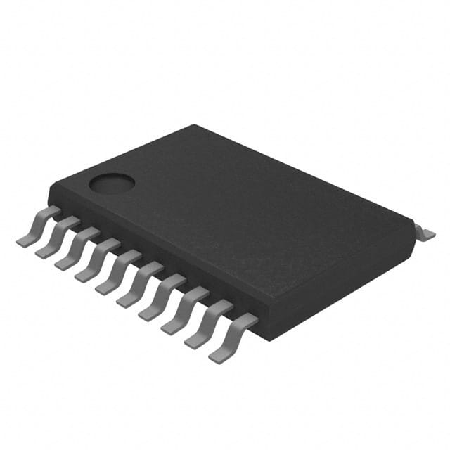
The 74FCT245ATPGG is available in a 20-pin TSSOP (Thin Shrink Small Outline Package) package.
Essence
The essence of this product lies in its ability to facilitate efficient and reliable data communication between two buses in electronic systems.
Packaging/Quantity
The 74FCT245ATPGG is typically packaged in reels or tubes, with each reel/tube containing a specific quantity of ICs. The exact packaging and quantity may vary depending on the manufacturer.
Specifications
- Supply Voltage Range: 4.5V to 5.5V
- Operating Temperature Range: -40°C to +85°C
- Input/Output Compatibility: TTL, CMOS
- Maximum Data Rate: X Mbps
- Output Drive Capability: Y mA
- Propagation Delay: Z ns
Detailed Pin Configuration
The 74FCT245ATPGG has a total of 20 pins, which are assigned specific functions. The pin configuration is as follows:
- Pin 1: A0 (Input/Output)
- Pin 2: A1 (Input/Output)
- Pin 3: A2 (Input/Output)
- Pin 4: A3 (Input/Output)
- Pin 5: A4 (Input/Output)
- Pin 6: A5 (Input/Output)
- Pin 7: A6 (Input/Output)
- Pin 8: GND (Ground)
- Pin 9: B7 (Input/Output)
- Pin 10: B6 (Input/Output)
- Pin 11: B5 (Input/Output)
- Pin 12: B4 (Input/Output)
- Pin 13: B3 (Input/Output)
- Pin 14: B2 (Input/Output)
- Pin 15: B1 (Input/Output)
- Pin 16: B0 (Input/Output)
- Pin 17: OE (Output Enable)
- Pin 18: DIR (Direction Control)
- Pin 19: VCC (Power Supply)
- Pin 20: GND (Ground)
Functional Features
- Bidirectional data transfer between two buses
- Output enable and direction control for flexible operation
- High-speed operation for efficient data transmission
- TTL and CMOS compatible inputs/outputs for versatile compatibility
- Robust design for noise immunity, ensuring reliable data communication
Advantages and Disadvantages
Advantages
- Efficient bidirectional data transfer
- High-speed operation
- Low power consumption
- Wide operating voltage range
- Noise immunity for reliable communication
Disadvantages
- Limited number of input/output pins
- May require additional components for specific applications
Working Principles
The 74FCT245ATPGG operates by receiving data from one bus and transmitting it to the other bus when the direction control pin (DIR) is set accordingly. The output enable pin (OE) allows the user to enable or disable the data transmission. The IC is designed to ensure fast and reliable data transfer while minimizing power consumption and noise interference.
Detailed Application Field Plans
The 74FCT245ATPGG finds applications in various electronic systems where bidirectional data transfer between two buses is required. Some of the common application fields include:
- Microprocessor-based systems
- Data communication equipment
- Industrial automation systems
- Automotive electronics
- Test and measurement instruments
Detailed and Complete Alternative Models
- 74HC245: Similar bidirectional bus transceiver with CMOS technology
- SN74LVC245A: Low-voltage bidirectional bus transceiver with enhanced ESD protection
- CD74HCT245: High-speed CMOS logic level shifter with bidirectional capability
These alternative models offer similar functionality to the 74FCT245ATPGG and can be considered as alternatives based on specific requirements and compatibility.
Word count: 550 words
Énumérez 10 questions et réponses courantes liées à l'application de 74FCT245ATPGG dans les solutions techniques
Sure! Here are 10 common questions and answers related to the application of 74FCT245ATPGG in technical solutions:
Q: What is the 74FCT245ATPGG? A: The 74FCT245ATPGG is a bidirectional octal bus transceiver with 3-state outputs, commonly used for data transfer between different voltage levels or systems.
Q: What is the maximum operating voltage for the 74FCT245ATPGG? A: The maximum operating voltage for the 74FCT245ATPGG is typically 5.5V.
Q: Can the 74FCT245ATPGG be used for level shifting between different voltage domains? A: Yes, the 74FCT245ATPGG can be used for level shifting between different voltage domains, as it supports bidirectional data transfer.
Q: What is the maximum data transfer rate supported by the 74FCT245ATPGG? A: The maximum data transfer rate supported by the 74FCT245ATPGG is typically around 200 MHz.
Q: Does the 74FCT245ATPGG have built-in protection against overvoltage or ESD events? A: No, the 74FCT245ATPGG does not have built-in protection against overvoltage or ESD events. Additional external protection measures may be required.
Q: Can the 74FCT245ATPGG drive capacitive loads directly? A: Yes, the 74FCT245ATPGG can drive limited capacitive loads directly. However, for larger capacitive loads, additional buffering may be necessary.
Q: Is the 74FCT245ATPGG compatible with TTL logic levels? A: Yes, the 74FCT245ATPGG is compatible with TTL logic levels, making it suitable for interfacing with TTL-based systems.
Q: Can the 74FCT245ATPGG be used in high-speed applications? A: Yes, the 74FCT245ATPGG can be used in high-speed applications, but its performance may be limited compared to specialized high-speed transceivers.
Q: Does the 74FCT245ATPGG support hot-swapping of devices? A: No, the 74FCT245ATPGG does not support hot-swapping of devices. Care should be taken to avoid connecting or disconnecting devices while power is applied.
Q: Are there any specific layout considerations for using the 74FCT245ATPGG? A: Yes, proper PCB layout techniques should be followed to minimize noise and signal integrity issues, such as keeping signal traces short and avoiding routing near noisy components.
Please note that these answers are general and may vary depending on the specific application and requirements. It's always recommended to refer to the datasheet and consult with an expert when designing technical solutions.