

Voir les spécifications pour les détails du produit.
PI6C485352FAE
Overview
- Category: Integrated Circuit
- Use: Clock Generator and Buffer
- Characteristics:
- Low jitter
- Wide frequency range
- High accuracy
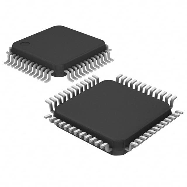
- Package: QFN (Quad Flat No-leads)
- Essence: Clock generation and buffering
- Packaging/Quantity: Tape and Reel, 2500 units per reel
Specifications and Parameters
- Input Voltage Range: 2.5V to 3.3V
- Output Frequency Range: 1MHz to 200MHz
- Output Type: LVCMOS
- Operating Temperature Range: -40°C to +85°C
- Supply Current: 20mA (typical)
Pin Configuration
The PI6C485352FAE has a total of 32 pins arranged as follows:
1   2   3   4   5   6   7   8   9   10
+---+---+---+---+---+---+---+---+---+---+
|   |   |   |   |   |   |   |   |   |   |
|   |   |   |   |   |   |   |   |   |   |
+---+---+---+---+---+---+---+---+---+---+
  11  12  13  14  15  16  17  18  19  20
Functional Characteristics
The PI6C485352FAE is designed to generate and buffer clock signals with low jitter and high accuracy. It provides a wide frequency range from 1MHz to 200MHz, making it suitable for various applications requiring precise timing.
Advantages and Disadvantages
Advantages: - Low jitter for accurate timing - Wide frequency range for versatile applications - High accuracy for reliable performance
Disadvantages: - Limited output voltage options (LVCMOS only) - Relatively high supply current compared to some alternatives
Applicable Range of Products
The PI6C485352FAE is commonly used in electronic devices that require clock generation and buffering, such as communication equipment, computer systems, and consumer electronics.
Working Principles
The PI6C485352FAE utilizes internal circuitry to generate clock signals based on the input voltage and frequency settings. It then buffers the generated signals to ensure stable and accurate timing throughout the system.
Detailed Application Field Plans
- Communication Equipment: The PI6C485352FAE can be used in routers, switches, and network cards to provide precise clock synchronization for data transmission.
- Computer Systems: It can be employed in motherboards, graphics cards, and storage devices to maintain accurate timing for various operations.
- Consumer Electronics: The IC can be integrated into TVs, set-top boxes, and gaming consoles to synchronize audio and video signals.
Detailed Alternative Models
- PI6C485351FAE: Similar to PI6C485352FAE but with a different pin configuration.
- PI6C485353FAE: Offers additional features such as frequency modulation and spread spectrum support.
5 Common Technical Questions and Answers
Q: What is the maximum output frequency of PI6C485352FAE? A: The maximum output frequency is 200MHz.
Q: Can I use this IC with a 5V power supply? A: No, the recommended input voltage range is 2.5V to 3.3V.
Q: Does PI6C485352FAE support differential outputs? A: No, it only provides LVCMOS output type.
Q: What is the operating temperature range of this IC? A: It can operate within -40°C to +85°C.
Q: How many units are there in a standard reel packaging? A: The standard reel packaging contains 2500 units.
This encyclopedia entry provides an overview of the PI6C485352FAE, including its basic information, specifications, pin configuration, functional characteristics, advantages and disadvantages, applicable range of products, working principles, detailed application field plans, alternative models, and common technical questions and answers.