

Voir les spécifications pour les détails du produit.
Encyclopedia Entry: 74LVC573AQ20-13
Product Overview
Category
The 74LVC573AQ20-13 belongs to the category of integrated circuits (ICs).
Use
This IC is commonly used in digital electronic systems for data storage and transfer.
Characteristics
- Low-voltage CMOS technology
- High-speed operation
- Wide operating voltage range
- Schmitt-trigger action on all inputs
- 3-state outputs for bus-oriented applications
Package
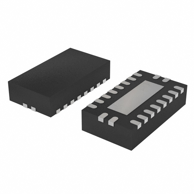
The 74LVC573AQ20-13 is available in a 20-pin TSSOP package.
Essence
The essence of this product lies in its ability to store and transfer digital data efficiently within electronic systems.
Packaging/Quantity
The 74LVC573AQ20-13 is typically packaged in reels or tubes, with a quantity of 250 units per reel/tube.
Specifications
- Supply Voltage Range: 1.2V to 3.6V
- Input Voltage Range: -0.5V to VCC + 0.5V
- Output Voltage Range: -0.5V to VCC + 0.5V
- Operating Temperature Range: -40°C to +85°C
- Maximum Clock Frequency: 100 MHz
Detailed Pin Configuration
The 74LVC573AQ20-13 has a total of 20 pins, each serving a specific function. The pin configuration is as follows:
- GND (Ground)
- D0 (Data Input 0)
- D1 (Data Input 1)
- D2 (Data Input 2)
- D3 (Data Input 3)
- D4 (Data Input 4)
- D5 (Data Input 5)
- D6 (Data Input 6)
- D7 (Data Input 7)
- OE (Output Enable)
- LE (Latch Enable)
- Q0 (Output 0)
- Q1 (Output 1)
- Q2 (Output 2)
- Q3 (Output 3)
- Q4 (Output 4)
- Q5 (Output 5)
- Q6 (Output 6)
- Q7 (Output 7)
- VCC (Supply Voltage)
Functional Features
The 74LVC573AQ20-13 offers the following functional features:
- 8-bit transparent latch with 3-state outputs
- Non-inverting outputs for direct interfacing with other digital components
- Schmitt-trigger inputs for improved noise immunity
- Output enable and latch enable control for flexible data transfer
Advantages and Disadvantages
Advantages
- Low-voltage operation allows compatibility with a wide range of systems
- High-speed operation enables efficient data transfer
- Schmitt-trigger action on inputs enhances noise immunity
- 3-state outputs facilitate bus-oriented applications
Disadvantages
- Limited maximum clock frequency of 100 MHz may restrict use in high-speed applications
- Availability in only TSSOP package may limit compatibility with certain system designs
Working Principles
The 74LVC573AQ20-13 operates based on the principles of CMOS technology. It utilizes latches to store and transfer digital data. The latch enable (LE) signal controls the storage of data, while the output enable (OE) signal determines whether the outputs are active or in a high-impedance state.
Detailed Application Field Plans
The 74LVC573AQ20-13 finds extensive application in various digital electronic systems, including but not limited to: - Microcontrollers - Data communication devices - Memory modules - Industrial automation systems - Consumer electronics
Detailed and Complete Alternative Models
- 74HC573: Similar functionality, but operates at higher voltage levels (2V to 6V)
- 74ACT573: Faster operation with a maximum clock frequency of 200 MHz
- SN74LVC573A: Equivalent IC from Texas Instruments with similar specifications and features
In conclusion, the 74LVC573AQ20-13 is a versatile integrated circuit used for data storage and transfer in digital electronic systems. Its low-voltage CMOS technology, high-speed operation, and 3-state outputs make it suitable for various applications. However, its limited clock frequency and package options should be considered when selecting alternative models.
Énumérez 10 questions et réponses courantes liées à l'application de 74LVC573AQ20-13 dans les solutions techniques
Sure! Here are 10 common questions and answers related to the application of 74LVC573AQ20-13 in technical solutions:
Q: What is the 74LVC573AQ20-13? A: The 74LVC573AQ20-13 is a octal transparent latch with 3-state outputs, designed for low-voltage applications.
Q: What is the operating voltage range of the 74LVC573AQ20-13? A: The operating voltage range is from 1.65V to 5.5V.
Q: How many latch outputs does the 74LVC573AQ20-13 have? A: It has 8 latch outputs.
Q: What is the maximum output current of the 74LVC573AQ20-13? A: The maximum output current is 32mA.
Q: Can the 74LVC573AQ20-13 be used in high-speed applications? A: Yes, it has a maximum propagation delay of 6.5ns, making it suitable for high-speed applications.
Q: Does the 74LVC573AQ20-13 have internal pull-up or pull-down resistors? A: No, it does not have internal pull-up or pull-down resistors.
Q: Can the 74LVC573AQ20-13 be used in bidirectional data transfer? A: No, it is a unidirectional latch and does not support bidirectional data transfer.
Q: What is the power supply current of the 74LVC573AQ20-13? A: The power supply current is typically 2.5mA.
Q: Is the 74LVC573AQ20-13 compatible with other logic families? A: Yes, it is compatible with both TTL and CMOS logic families.
Q: Can the 74LVC573AQ20-13 be used in automotive applications? A: Yes, it is AEC-Q100 qualified and suitable for automotive applications.
Please note that these answers are general and may vary depending on the specific application and conditions. It is always recommended to refer to the datasheet and consult with the manufacturer for detailed information.