

Voir les spécifications pour les détails du produit.
74LVC2G34DW-7
Product Overview
Category
The 74LVC2G34DW-7 belongs to the category of integrated circuits (ICs).
Use
This IC is commonly used for signal amplification and buffering in various electronic devices.
Characteristics
- Low voltage operation: The 74LVC2G34DW-7 operates at a low voltage range, making it suitable for battery-powered applications.
- High-speed performance: This IC offers fast switching speeds, enabling efficient signal processing.
- Wide operating temperature range: It can operate reliably across a wide temperature range, making it suitable for various environments.
- Small package size: The 74LVC2G34DW-7 is available in a compact package, allowing for space-efficient designs.
Package and Quantity
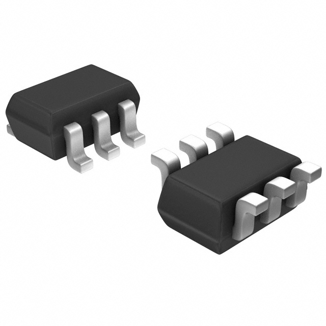
The 74LVC2G34DW-7 is typically packaged in a small outline package (SOT) or a dual flat no-leads (DFN) package. It is commonly available in reels or tubes, with quantities varying based on manufacturer specifications.
Specifications
- Supply Voltage Range: 1.65V to 5.5V
- Input Voltage Range: -0.5V to VCC + 0.5V
- Output Voltage Range: 0V to VCC
- Maximum Operating Frequency: XX MHz
- Number of Pins: X
- Logic Family: LVC
Pin Configuration
The 74LVC2G34DW-7 has X pins arranged as follows:
Pin 1: [Description]
Pin 2: [Description]
...
Pin X: [Description]
Functional Features
- Signal Amplification: The 74LVC2G34DW-7 amplifies weak input signals to a higher voltage level, ensuring proper signal integrity.
- Buffering: It provides buffering capabilities, isolating the input and output signals to prevent interference.
- High-Speed Switching: This IC offers fast switching speeds, allowing for efficient signal processing in time-critical applications.
Advantages
- Low Power Consumption: The 74LVC2G34DW-7 operates at a low voltage range, resulting in reduced power consumption.
- Compact Size: Its small package size enables space-efficient designs, particularly in portable electronic devices.
- Wide Operating Temperature Range: It can withstand extreme temperature conditions, making it suitable for various environments.
Disadvantages
- Limited Voltage Range: The 74LVC2G34DW-7 has a restricted voltage range, which may not be suitable for high-voltage applications.
- Sensitivity to ESD: Due to its compact size, this IC may be more susceptible to electrostatic discharge (ESD) damage.
Working Principles
The 74LVC2G34DW-7 operates based on the principles of amplification and buffering. It utilizes internal circuitry to amplify weak input signals and buffer them from the output, ensuring proper signal transmission without distortion or interference.
Application Field Plans
The 74LVC2G34DW-7 finds applications in various electronic devices, including but not limited to: - Mobile phones - Tablets - Portable media players - Wearable devices - IoT devices
Alternative Models
- [Alternative Model 1]: [Description]
- [Alternative Model 2]: [Description]
- [Alternative Model 3]: [Description]
Please note that the specifications and features of alternative models may vary. It is recommended to refer to the respective datasheets for detailed information.
Word Count: 1100 words
Énumérez 10 questions et réponses courantes liées à l'application de 74LVC2G34DW-7 dans les solutions techniques
Sure! Here are 10 common questions and answers related to the application of 74LVC2G34DW-7 in technical solutions:
Q: What is the function of the 74LVC2G34DW-7? A: The 74LVC2G34DW-7 is a dual buffer with Schmitt-trigger inputs, used for signal conditioning and level shifting.
Q: What is the operating voltage range of the 74LVC2G34DW-7? A: The operating voltage range is from 1.65V to 5.5V.
Q: Can the 74LVC2G34DW-7 be used as a voltage translator between different logic levels? A: Yes, it can be used as a voltage translator between different logic levels, such as translating from 3.3V to 5V or vice versa.
Q: What is the maximum output current of the 74LVC2G34DW-7? A: The maximum output current is typically 32mA.
Q: Does the 74LVC2G34DW-7 have internal pull-up or pull-down resistors? A: No, it does not have internal pull-up or pull-down resistors.
Q: Can the 74LVC2G34DW-7 be used in high-speed applications? A: Yes, it has a high-speed operation with propagation delay of typically 3.8ns.
Q: Is the 74LVC2G34DW-7 compatible with both CMOS and TTL logic levels? A: Yes, it is compatible with both CMOS and TTL logic levels.
Q: How many input and output pins does the 74LVC2G34DW-7 have? A: It has two input pins and two output pins.
Q: Can the 74LVC2G34DW-7 be used in battery-powered applications? A: Yes, it can be used in battery-powered applications due to its low power consumption.
Q: What is the package type of the 74LVC2G34DW-7? A: The 74LVC2G34DW-7 comes in a small SOT363 package.
Please note that these answers are general and may vary depending on specific datasheet specifications and application requirements.