

Voir les spécifications pour les détails du produit.
Encyclopedia Entry: 74LVC1G06SE-7
Product Overview
Category
The 74LVC1G06SE-7 belongs to the category of integrated circuits (ICs) and specifically falls under the family of logic gates.
Use
This product is commonly used in digital electronics for signal inversion and buffering purposes. It acts as a single inverter gate, converting input signals into their complementary form.
Characteristics
- Low-voltage CMOS technology
- High-speed operation
- Wide operating voltage range
- Schmitt-trigger action on inputs
- Balanced propagation delays
- Low power consumption
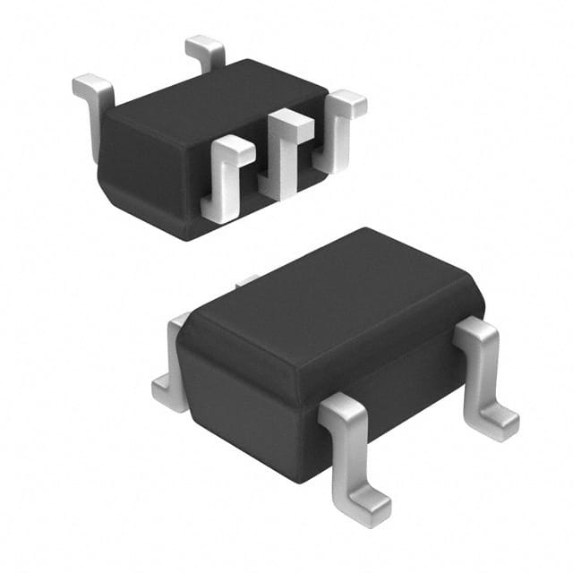
Package
The 74LVC1G06SE-7 is available in a small SOT-353 package, which is a surface-mount package with three leads.
Essence
The essence of this product lies in its ability to provide reliable and efficient signal inversion functionality in various digital applications.
Packaging/Quantity
The 74LVC1G06SE-7 is typically packaged in reels or tubes, containing a specific quantity of ICs per package. The exact packaging and quantity may vary depending on the manufacturer.
Specifications
- Supply Voltage Range: 1.65V to 5.5V
- Input Voltage Range: -0.5V to VCC + 0.5V
- Output Voltage Range: -0.5V to VCC + 0.5V
- Maximum Operating Frequency: 200 MHz
- Maximum Propagation Delay: 4.3 ns
- Operating Temperature Range: -40°C to +125°C
Detailed Pin Configuration
The 74LVC1G06SE-7 has three pins: 1. GND (Ground): Connected to the ground reference of the circuit. 2. IN (Input): Receives the input signal to be inverted. 3. OUT (Output): Provides the inverted output signal.
Functional Features
- Signal inversion: The input signal is inverted and provided as the output.
- Schmitt-trigger action: Ensures a clean and stable output even in the presence of noisy or slowly changing input signals.
- Balanced propagation delays: Minimizes timing discrepancies between multiple gates in a circuit.
Advantages
- Low power consumption: Ideal for battery-powered devices and energy-efficient applications.
- Wide operating voltage range: Allows compatibility with various voltage levels.
- High-speed operation: Enables fast signal processing and reduces overall system latency.
- Small package size: Saves board space and facilitates compact designs.
Disadvantages
- Single gate functionality: Limited to signal inversion and does not provide other logic functions.
- SOT-353 package: Surface-mount package may require specialized equipment for soldering and rework.
Working Principles
The 74LVC1G06SE-7 utilizes CMOS technology to achieve signal inversion. When the input signal is high, the output is low, and vice versa. The Schmitt-trigger action ensures that the output transitions occur at well-defined voltage thresholds, improving noise immunity and signal integrity.
Detailed Application Field Plans
The 74LVC1G06SE-7 finds applications in various digital systems, including: - Microcontrollers and microprocessors - Communication systems - Industrial automation - Consumer electronics - Automotive electronics
Detailed Alternative Models
- 74LVC1G04SE-7: Hex inverter gate with similar characteristics and package.
- 74LVC1G07SE-7: Single buffer gate with open-drain output.
- 74LVC1G08SE-7: Single AND gate with Schmitt-trigger inputs.
In conclusion, the 74LVC1G06SE-7 is a versatile and efficient single inverter gate used in digital electronics. Its low power consumption, high-speed operation, and wide voltage range make it suitable for various applications. However, its limited functionality and specialized package may pose some limitations.
Énumérez 10 questions et réponses courantes liées à l'application de 74LVC1G06SE-7 dans les solutions techniques
Sure! Here are 10 common questions and answers related to the application of 74LVC1G06SE-7 in technical solutions:
Q1: What is the 74LVC1G06SE-7? A1: The 74LVC1G06SE-7 is a single gate buffer/inverter with open-drain output, commonly used in digital logic circuits.
Q2: What is the voltage supply range for the 74LVC1G06SE-7? A2: The voltage supply range for the 74LVC1G06SE-7 is typically between 1.65V and 5.5V.
Q3: What is the maximum output current of the 74LVC1G06SE-7? A3: The maximum output current of the 74LVC1G06SE-7 is 32mA.
Q4: Can the 74LVC1G06SE-7 be used as a level shifter? A4: Yes, the 74LVC1G06SE-7 can be used as a level shifter to convert signals between different voltage levels.
Q5: What is the propagation delay of the 74LVC1G06SE-7? A5: The propagation delay of the 74LVC1G06SE-7 is typically around 4.3ns.
Q6: Is the 74LVC1G06SE-7 suitable for high-speed applications? A6: Yes, the 74LVC1G06SE-7 is designed for high-speed operation and can be used in applications requiring fast switching times.
Q7: Can the 74LVC1G06SE-7 drive capacitive loads? A7: Yes, the 74LVC1G06SE-7 can drive capacitive loads up to a certain limit, typically around 50pF.
Q8: What is the input voltage threshold for the 74LVC1G06SE-7? A8: The input voltage threshold for the 74LVC1G06SE-7 is typically around 0.8V.
Q9: Can the 74LVC1G06SE-7 be used in battery-powered applications? A9: Yes, the 74LVC1G06SE-7 has a low power consumption and can be used in battery-powered applications.
Q10: Is the 74LVC1G06SE-7 available in different package options? A10: Yes, the 74LVC1G06SE-7 is available in various package options, such as SOT23 and SC70.
Please note that these answers are general and may vary depending on specific datasheet specifications and application requirements.