

Voir les spécifications pour les détails du produit.
CY7B9334-270JXCT
Product Overview
Category
CY7B9334-270JXCT belongs to the category of integrated circuits (ICs).
Use
This product is commonly used in electronic devices for signal transmission and processing.
Characteristics
- High-speed performance
- Low power consumption
- Compact size
- Reliable operation
Package
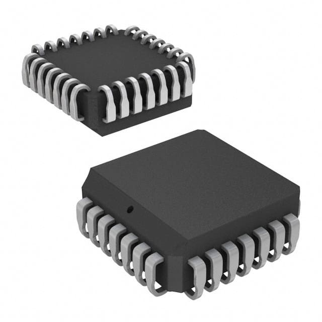
CY7B9334-270JXCT is available in a small form factor package, which allows for easy integration into various electronic systems.
Essence
The essence of CY7B9334-270JXCT lies in its ability to efficiently transmit and process signals in electronic devices.
Packaging/Quantity
This product is typically packaged in reels or tubes, with a quantity of 1000 units per package.
Specifications
- Model: CY7B9334-270JXCT
- Operating Voltage: 3.3V
- Frequency Range: Up to 270 MHz
- Number of Pins: 32
- Input/Output Logic Levels: CMOS/TTL compatible
- Operating Temperature Range: -40°C to +85°C
Detailed Pin Configuration
- VDD
- GND
- CLK_IN
- CLK_OUT
- OE
- Q0
- Q1
- Q2
- Q3
- Q4
- Q5
- Q6
- Q7
- Q8
- Q9
- Q10
- Q11
- Q12
- Q13
- Q14
- Q15
- Q16
- Q17
- Q18
- Q19
- Q20
- Q21
- Q22
- Q23
- Q24
- Q25
- Q26
Functional Features
- High-speed clock distribution
- Low jitter and skew
- Wide operating frequency range
- Output enable control for power management
- Multiple output channels for signal distribution
Advantages and Disadvantages
Advantages
- High-speed performance enables efficient signal transmission
- Low power consumption contributes to energy efficiency
- Compact size allows for easy integration into electronic systems
- Reliable operation ensures stable signal processing
Disadvantages
- Limited number of output channels may restrict certain applications
- Higher cost compared to some alternative models
Working Principles
CY7B9334-270JXCT operates by receiving an input clock signal (CLK_IN) and distributing it to multiple output channels (Q0-Q26). The output enable (OE) pin controls the activation of the output channels. The integrated circuit utilizes advanced technology to ensure high-speed, low-jitter, and low-skew clock distribution.
Detailed Application Field Plans
CY7B9334-270JXCT finds application in various electronic devices and systems, including: 1. Communication equipment 2. Networking devices 3. Data storage systems 4. Industrial automation 5. Test and measurement instruments
Detailed and Complete Alternative Models
- CY7B9334-200JXCT: Similar to CY7B9334-270JXCT but with a lower operating frequency of up to 200 MHz.
- CY7B9334-400JXCT: Similar to CY7B9334-270JXCT but with a higher operating frequency of up to 400 MHz.
- CY7B9334-270JXC: Same operating frequency as CY7B9334-270JXCT but without the extended temperature range.
These alternative models provide options based on specific requirements and operating conditions.
Word count: 446 words
Énumérez 10 questions et réponses courantes liées à l'application de CY7B9334-270JXCT dans les solutions techniques
Sure! Here are 10 common questions and answers related to the application of CY7B9334-270JXCT in technical solutions:
Question: What is the CY7B9334-270JXCT?
Answer: The CY7B9334-270JXCT is a specific model of a clock generator IC (integrated circuit) manufactured by Cypress Semiconductor.Question: What is the purpose of the CY7B9334-270JXCT?
Answer: The CY7B9334-270JXCT is designed to generate precise clock signals for various electronic devices and systems.Question: What are the key features of the CY7B9334-270JXCT?
Answer: Some key features include a wide frequency range, low jitter performance, multiple output options, and programmable settings.Question: In which applications can the CY7B9334-270JXCT be used?
Answer: The CY7B9334-270JXCT can be used in a wide range of applications such as networking equipment, telecommunications, data centers, and industrial automation.Question: How does the CY7B9334-270JXCT help in improving system performance?
Answer: By providing accurate and stable clock signals, the CY7B9334-270JXCT helps in synchronizing different components of a system, reducing timing errors, and improving overall performance.Question: Can the CY7B9334-270JXCT be programmed for specific frequency requirements?
Answer: Yes, the CY7B9334-270JXCT offers programmable settings that allow users to configure the desired frequency and other parameters.Question: What is the power supply requirement for the CY7B9334-270JXCT?
Answer: The CY7B9334-270JXCT typically operates on a 3.3V power supply, but it is always recommended to refer to the datasheet for specific details.Question: Does the CY7B9334-270JXCT support multiple output formats?
Answer: Yes, the CY7B9334-270JXCT supports various output formats such as LVPECL, LVDS, and HCSL, making it compatible with different system requirements.Question: Are there any design considerations when using the CY7B9334-270JXCT?
Answer: Yes, it is important to consider factors like board layout, signal integrity, and proper decoupling to ensure optimal performance when integrating the CY7B9334-270JXCT into a design.Question: Where can I find more information about the CY7B9334-270JXCT?
Answer: You can find detailed information, including datasheets, application notes, and technical support, on the official website of Cypress Semiconductor or by contacting their customer support team.