Voir les spécifications pour les détails du produit.

CY241V8ASXC-12T
Product Overview
Category
CY241V8ASXC-12T belongs to the category of integrated circuits (ICs).
Use
This product is primarily used for signal conditioning and clock distribution in electronic devices.
Characteristics
- Signal conditioning capabilities
- Clock distribution functionality
- High performance and reliability
- Compact size
- Low power consumption
Package
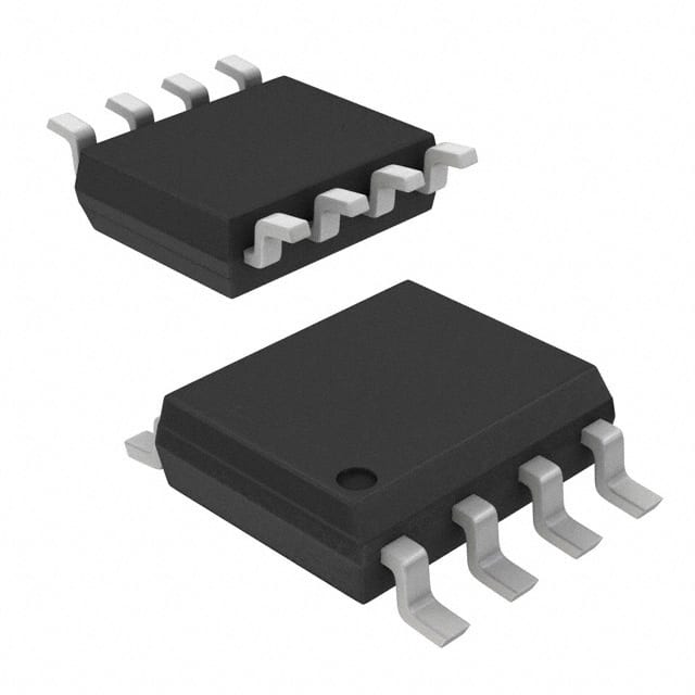
The CY241V8ASXC-12T is available in a small outline integrated circuit (SOIC) package.
Essence
The essence of CY241V8ASXC-12T lies in its ability to condition signals and distribute clocks efficiently within electronic systems.
Packaging/Quantity
The product is typically packaged in reels or tubes, with each containing a specific quantity of ICs. The exact quantity may vary depending on the manufacturer's specifications.
Specifications
- Model: CY241V8ASXC-12T
- Operating Voltage: 3.3V
- Frequency Range: Up to 100 MHz
- Number of Pins: 12
- Output Type: LVCMOS
- Operating Temperature Range: -40°C to +85°C
Detailed Pin Configuration
- VDD
- GND
- CLKIN
- CLKOUT0
- CLKOUT1
- CLKOUT2
- CLKOUT3
- CLKOUT4
- CLKOUT5
- CLKOUT6
- CLKOUT7
- NC
Functional Features
- Signal conditioning: The CY241V8ASXC-12T can amplify, filter, or shape input signals to ensure optimal performance.
- Clock distribution: It can distribute a single clock signal to multiple output channels with minimal skew and jitter.
- Output enable control: The device allows individual output channels to be enabled or disabled as per the system requirements.
- Low power consumption: The IC is designed to operate with low power consumption, making it suitable for battery-powered devices.
Advantages and Disadvantages
Advantages
- High-performance signal conditioning and clock distribution capabilities
- Compact size allows for easy integration into various electronic systems
- Reliable operation in a wide temperature range
- Low power consumption prolongs battery life in portable devices
Disadvantages
- Limited number of output channels (8 in this case)
- May require additional external components for specific applications
Working Principles
The CY241V8ASXC-12T operates by receiving an input clock signal (CLKIN) and conditioning it using internal circuitry. The conditioned clock signal is then distributed to the output channels (CLKOUT0-CLKOUT7) with minimal skew and jitter. The device also provides output enable control, allowing individual output channels to be enabled or disabled based on system requirements.
Detailed Application Field Plans
The CY241V8ASXC-12T finds application in various electronic systems, including but not limited to: - Communication equipment - Computer peripherals - Consumer electronics - Industrial automation - Medical devices
Detailed and Complete Alternative Models
- CY241V8ASXC-10T: Similar to CY241V8ASXC-12T, but with 10 output channels instead of 8.
- CY241V8ASXC-14T: Similar to CY241V8ASXC-12T, but with 14 output channels instead of 8.
- CY241V8ASXC-16T: Similar to CY241V8ASXC-12T, but with 16 output channels instead of 8.
These alternative models offer similar functionality with varying numbers of output channels, providing flexibility for different system requirements.
In conclusion, the CY241V8ASXC-12T is a versatile integrated circuit that excels in signal conditioning and clock distribution applications. Its compact size, low power consumption, and reliable performance make it suitable for a wide range of electronic devices across various industries.
Énumérez 10 questions et réponses courantes liées à l'application de CY241V8ASXC-12T dans les solutions techniques
Sure! Here are 10 common questions and answers related to the application of CY241V8ASXC-12T in technical solutions:
1. What is the CY241V8ASXC-12T? The CY241V8ASXC-12T is a specific model of a programmable clock generator integrated circuit (IC) manufactured by Cypress Semiconductor.
2. What is the purpose of the CY241V8ASXC-12T? The CY241V8ASXC-12T is designed to generate precise clock signals for various electronic systems, such as microprocessors, digital signal processors, and other timing-critical applications.
3. What is the operating frequency range of the CY241V8ASXC-12T? The CY241V8ASXC-12T operates within a frequency range of 1 MHz to 200 MHz.
4. How many output clocks can the CY241V8ASXC-12T generate? The CY241V8ASXC-12T can generate up to eight different output clocks.
5. Can the output frequencies be programmed on the CY241V8ASXC-12T? Yes, the output frequencies can be programmed using the device's configuration pins or through an I2C interface.
6. What is the power supply voltage requirement for the CY241V8ASXC-12T? The CY241V8ASXC-12T requires a power supply voltage of 3.3V.
7. Does the CY241V8ASXC-12T support spread spectrum clocking (SSC)? Yes, the CY241V8ASXC-12T supports spread spectrum clocking, which helps reduce electromagnetic interference (EMI).
8. Can the CY241V8ASXC-12T be used in automotive applications? Yes, the CY241V8ASXC-12T is qualified for automotive applications and meets the necessary industry standards.
9. What are the available package options for the CY241V8ASXC-12T? The CY241V8ASXC-12T is available in a small footprint 20-pin TSSOP package.
10. Are there any evaluation boards or reference designs available for the CY241V8ASXC-12T? Yes, Cypress Semiconductor provides evaluation boards and reference designs to help users quickly prototype and integrate the CY241V8ASXC-12T into their technical solutions.
Please note that the specific details mentioned above may vary, so it's always recommended to refer to the official documentation and datasheet provided by the manufacturer for accurate information.

