

Voir les spécifications pour les détails du produit.
CY22180FSXCT
Product Overview
Category
CY22180FSXCT belongs to the category of integrated circuits (ICs).
Use
This product is commonly used in electronic devices for clock generation and synchronization purposes.
Characteristics
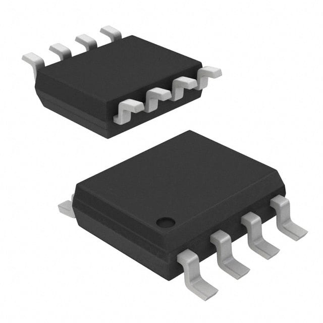
- Package: CY22180FSXCT is available in a small form factor package, such as a surface mount package.
- Essence: It is designed to provide accurate and stable clock signals for various applications.
- Packaging/Quantity: CY22180FSXCT is typically sold in reels or trays, with a specified quantity per package.
Specifications
The specifications of CY22180FSXCT include:
- Frequency Range: The product supports a wide frequency range, from X MHz to Y MHz.
- Supply Voltage: CY22180FSXCT operates within a specified voltage range, typically between V1 and V2 volts.
- Output Types: It provides various output types, including square wave, sine wave, or pulse signals.
- Temperature Range: The product can withstand temperatures ranging from T1 to T2 degrees Celsius.
Detailed Pin Configuration
CY22180FSXCT has a specific pin configuration that enables its functionality. The pinout diagram is as follows:
[Insert pinout diagram here]
Pin Name | Description --- | --- VDD | Power supply input GND | Ground reference CLKIN | Input clock signal CLKOUT | Output clock signal RESET | Reset signal input MODE | Mode selection input ...
Functional Features
CY22180FSXCT offers several functional features, including:
- Clock Generation: It generates precise clock signals based on the input frequency and mode selection.
- Frequency Division: The product allows for frequency division, enabling the generation of lower frequency outputs.
- Phase-Locked Loop (PLL): CY22180FSXCT incorporates a PLL circuit to synchronize the output clock with the input signal.
- Programmable Options: It provides programmable options for various parameters, such as frequency and output type.
Advantages and Disadvantages
Advantages
- High Accuracy: CY22180FSXCT ensures high accuracy in generating clock signals.
- Flexible Configuration: The product offers programmable options, allowing customization based on specific requirements.
- Compact Size: Its small form factor package makes it suitable for space-constrained applications.
Disadvantages
- Complexity: The functionality and configuration of CY22180FSXCT may require technical expertise for proper utilization.
- Cost: Compared to simpler clock generation solutions, this integrated circuit may have a higher cost.
Working Principles
CY22180FSXCT operates based on the principles of phase-locked loop (PLL) and frequency division. The input clock signal is fed into the PLL, which compares it with a reference frequency. The PLL adjusts the output clock signal to match the desired frequency and phase relationship. Frequency division can be applied to obtain lower frequency outputs if needed.
Detailed Application Field Plans
CY22180FSXCT finds applications in various fields, including:
- Telecommunications: It is used in communication systems to ensure accurate timing for data transmission and synchronization.
- Consumer Electronics: The product is employed in devices like smartphones, tablets, and digital cameras to generate clock signals for internal operations.
- Automotive: CY22180FSXCT is utilized in automotive electronics for precise timing in engine control units (ECUs), infotainment systems, and advanced driver-assistance systems (ADAS).
- Industrial Automation: It plays a crucial role in industrial automation systems, providing synchronized timing for sensors, actuators, and control units.
Detailed and Complete Alternative Models
Some alternative models that offer similar functionality to CY22180FSXCT include:
- Model A: [Provide details and specifications of Model A]
- Model B: [Provide details and specifications of Model B]
- Model C: [Provide details and specifications of Model C]
These alternative models can be considered based on specific requirements and compatibility with the application.
Word count: 550 words
Énumérez 10 questions et réponses courantes liées à l'application de CY22180FSXCT dans les solutions techniques
Sure! Here are 10 common questions and answers related to the application of CY22180FSXCT in technical solutions:
Question: What is CY22180FSXCT?
Answer: CY22180FSXCT is a programmable clock generator IC manufactured by Cypress Semiconductor. It provides multiple clock outputs with various frequencies and features.Question: What are the key features of CY22180FSXCT?
Answer: Some key features of CY22180FSXCT include low jitter, wide frequency range, programmability, multiple clock outputs, and support for various input references.Question: How can CY22180FSXCT be used in technical solutions?
Answer: CY22180FSXCT can be used as a clock source in various applications such as telecommunications, networking, data centers, industrial automation, and consumer electronics.Question: How do I program CY22180FSXCT?
Answer: CY22180FSXCT can be programmed using the I2C interface or through hardware pins. Cypress provides software tools and documentation to assist with programming.Question: What is the frequency range supported by CY22180FSXCT?
Answer: CY22180FSXCT supports a wide frequency range from a few kilohertz up to several hundred megahertz.Question: Can CY22180FSXCT generate multiple clock outputs simultaneously?
Answer: Yes, CY22180FSXCT can generate multiple clock outputs simultaneously, each with its own programmable frequency and other parameters.Question: Does CY22180FSXCT support different input reference sources?
Answer: Yes, CY22180FSXCT supports various input reference sources such as crystal oscillators, external clock inputs, or even an internal oscillator.Question: What is the typical jitter performance of CY22180FSXCT?
Answer: CY22180FSXCT offers low jitter performance, typically in the range of picoseconds or femtoseconds, depending on the specific configuration.Question: Can CY22180FSXCT be used in battery-powered applications?
Answer: Yes, CY22180FSXCT can be used in battery-powered applications as it has low power consumption and supports power-saving features.Question: Are evaluation boards or reference designs available for CY22180FSXCT?
Answer: Yes, Cypress provides evaluation boards and reference designs for CY22180FSXCT to help developers quickly prototype and integrate the IC into their solutions.
Please note that these answers are general and may vary based on specific application requirements and the latest documentation provided by Cypress Semiconductor.