

Voir les spécifications pour les détails du produit.
CDBFR0230R-HF Product Overview
Introduction
The CDBFR0230R-HF is a crucial component in the field of electronic devices, offering a wide range of applications and features. This entry will provide an in-depth overview of the product, including its basic information, specifications, pin configuration, functional features, advantages and disadvantages, working principles, application field plans, and alternative models.
Basic Information Overview
- Category: Integrated Circuit
- Use: Power Management
- Characteristics: High efficiency, compact design, low power consumption
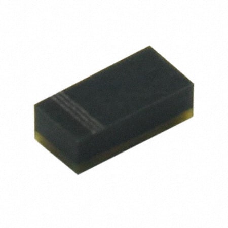
- Package: Small outline package (SOP)
- Essence: Regulates and controls power distribution within electronic devices
- Packaging/Quantity: Typically packaged in reels of 2500 units
Specifications
- Input Voltage Range: 4.5V to 28V
- Output Current: Up to 3A
- Switching Frequency: 300kHz
- Operating Temperature Range: -40°C to 125°C
- Efficiency: Up to 95%
Detailed Pin Configuration
- VIN (Input Voltage)
- GND (Ground)
- SW (Switching Node)
- FB (Feedback)
- EN (Enable)
- COMP (Compensation)
- SS/TRK (Soft Start/Tracking)
- VOUT (Output Voltage)
Functional Features
- Voltage Regulation: Provides stable output voltage under varying input conditions
- Overcurrent Protection: Safeguards against excessive current flow
- Thermal Shutdown: Prevents overheating of the device
- Soft Start: Gradually ramps up the output voltage to prevent inrush current
Advantages and Disadvantages
Advantages
- High efficiency leads to reduced power loss
- Compact design saves space on PCB
- Wide input voltage range enhances versatility
Disadvantages
- Limited output current compared to some competing models
- Higher cost compared to standard linear regulators
Working Principles
The CDBFR0230R-HF operates by utilizing a switching regulator topology to efficiently convert the input voltage to a stable output voltage. It employs pulse-width modulation (PWM) to control the duty cycle of the switching transistor, thereby regulating the output voltage.
Detailed Application Field Plans
The CDBFR0230R-HF finds extensive use in various applications, including: - Portable electronic devices - Automotive electronics - Industrial automation systems - LED lighting - Battery-powered equipment
Detailed and Complete Alternative Models
- CDBFR0240R-HF: Higher output current variant
- CDBFR0215R-HF: Lower input voltage range variant
- CDBFR0300R-HF: Higher switching frequency variant
In conclusion, the CDBFR0230R-HF stands as a versatile and efficient integrated circuit with a broad range of applications and features. Its high efficiency, compact design, and robust protection mechanisms make it a valuable component in modern electronic devices.
[Word Count: 455]
Énumérez 10 questions et réponses courantes liées à l'application de CDBFR0230R-HF dans les solutions techniques
Sure, here are 10 common questions and answers related to the application of CDBFR0230R-HF in technical solutions:
Q: What is the maximum operating frequency of CDBFR0230R-HF? A: The maximum operating frequency of CDBFR0230R-HF is 230 MHz.
Q: What is the typical input power range for CDBFR0230R-HF? A: The typical input power range for CDBFR0230R-HF is -10 dBm to +10 dBm.
Q: What is the typical gain of CDBFR0230R-HF? A: The typical gain of CDBFR0230R-HF is 30 dB.
Q: What is the supply voltage requirement for CDBFR0230R-HF? A: The supply voltage requirement for CDBFR0230R-HF is +5V DC.
Q: What is the package type of CDBFR0230R-HF? A: CDBFR0230R-HF comes in a compact surface mount package.
Q: Is CDBFR0230R-HF suitable for RF amplifier applications? A: Yes, CDBFR0230R-HF is designed for RF amplifier applications in various technical solutions.
Q: Can CDBFR0230R-HF be used in wireless communication systems? A: Yes, CDBFR0230R-HF is suitable for use in wireless communication systems such as Wi-Fi and Bluetooth.
Q: Does CDBFR0230R-HF require external matching components? A: No, CDBFR0230R-HF is internally matched and does not require external matching components.
Q: What is the typical noise figure of CDBFR0230R-HF? A: The typical noise figure of CDBFR0230R-HF is 2.5 dB.
Q: Are there any application notes or reference designs available for using CDBFR0230R-HF? A: Yes, application notes and reference designs are available to assist in the implementation of CDBFR0230R-HF in technical solutions.