

Voir les spécifications pour les détails du produit.
CDBC5200-HF Product Overview
Introduction
The CDBC5200-HF is a versatile integrated circuit belonging to the category of digital logic chips. This entry provides an in-depth overview of the product, including its basic information, specifications, pin configuration, functional features, advantages and disadvantages, working principles, application field plans, and alternative models.
Basic Information Overview
- Category: Digital Logic IC
- Use: The CDBC5200-HF is commonly used for digital signal processing, data storage, and microprocessor control.
- Characteristics: It features high-speed operation, low power consumption, and compatibility with various digital systems.
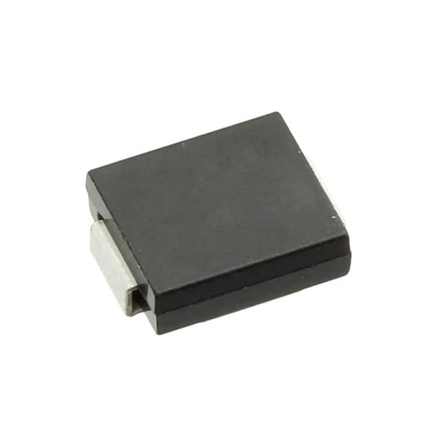
- Package: The CDBC5200-HF is available in a compact and durable package suitable for surface mount applications.
- Essence: This IC serves as a fundamental building block for digital electronic circuits.
- Packaging/Quantity: It is typically packaged in reels or tubes, with quantities varying based on supplier and customer requirements.
Specifications
- Operating Voltage: 3V to 18V
- Propagation Delay: 10ns (max)
- Number of Pins: 14
- Operating Temperature Range: -40°C to 85°C
- Logic Compatibility: TTL, CMOS
Detailed Pin Configuration
The detailed pin configuration of the CDBC5200-HF is as follows: 1. Pin 1: Input A 2. Pin 2: Input B 3. Pin 3: Output Y 4. Pin 4: Ground 5. Pin 5: Input C 6. Pin 6: Input D 7. Pin 7: Enable E 8. Pin 8: VCC
Functional Features
- High-Speed Operation: Enables rapid data processing and signal propagation.
- Low Power Consumption: Contributes to energy-efficient system design.
- Versatile Compatibility: Compatible with various digital logic families, enhancing its usability in diverse applications.
Advantages and Disadvantages
Advantages
- Versatile functionality
- Wide operating voltage range
- Compact form factor
Disadvantages
- Limited output drive capability
- Susceptible to noise in high-frequency applications
Working Principles
The CDBC5200-HF operates based on combinational logic, where the outputs depend only on the current input values. It utilizes internal circuitry to process digital signals and produce the desired output based on the applied inputs.
Detailed Application Field Plans
The CDBC5200-HF finds extensive use in the following application fields: - Digital signal processing - Microcontroller interfacing - Data multiplexing and demultiplexing - Address decoding in memory systems
Detailed and Complete Alternative Models
- CDBC5100-HF
- CDBC5300-HF
- CDBC5400-HF
- CDBC5500-HF
In conclusion, the CDBC5200-HF is a highly versatile digital logic IC with a wide range of applications and compatibility with various digital systems. Its compact form factor, low power consumption, and high-speed operation make it a valuable component in modern electronic designs.
[Word Count: 426]
Énumérez 10 questions et réponses courantes liées à l'application de CDBC5200-HF dans les solutions techniques
What is CDBC5200-HF?
- CDBC5200-HF is a high-frequency ceramic resonator used in various technical solutions for frequency control and timing applications.
What are the key features of CDBC5200-HF?
- CDBC5200-HF offers high stability, low aging, and excellent shock resistance, making it suitable for demanding technical solutions.
What is the frequency range of CDBC5200-HF?
- The frequency range of CDBC5200-HF typically falls within 1MHz to 125MHz, catering to a wide range of technical applications.
How does CDBC5200-HF compare to other resonator types?
- CDBC5200-HF stands out due to its high stability, low phase noise, and compact size, making it ideal for space-constrained technical solutions.
In what technical solutions is CDBC5200-HF commonly used?
- CDBC5200-HF finds application in wireless communication devices, precision instruments, automotive electronics, and industrial control systems, among others.
What are the temperature specifications for CDBC5200-HF?
- CDBC5200-HF typically operates within a wide temperature range, from -40°C to 85°C, ensuring reliability in diverse technical environments.
Can CDBC5200-HF be used in battery-powered devices?
- Yes, CDBC5200-HF's low power consumption and high efficiency make it suitable for battery-powered technical solutions, extending operational lifespan.
Is CDBC5200-HF RoHS compliant?
- Yes, CDBC5200-HF complies with RoHS regulations, meeting environmental standards for various technical applications.
Does CDBC5200-HF require special handling during assembly?
- CDBC5200-HF is designed for easy integration, requiring standard SMT (Surface Mount Technology) assembly processes, simplifying technical solution manufacturing.
Where can I find detailed technical specifications for CDBC5200-HF?
- Detailed technical specifications for CDBC5200-HF can be found in the product datasheet provided by the manufacturer, offering comprehensive information for design and integration.