

Voir les spécifications pour les détails du produit.
ADN2913ACPZ
Basic Information Overview
- Category: Integrated Circuit
- Use: Signal Conditioning and Amplification
- Characteristics: High-speed, Low-power, Precision
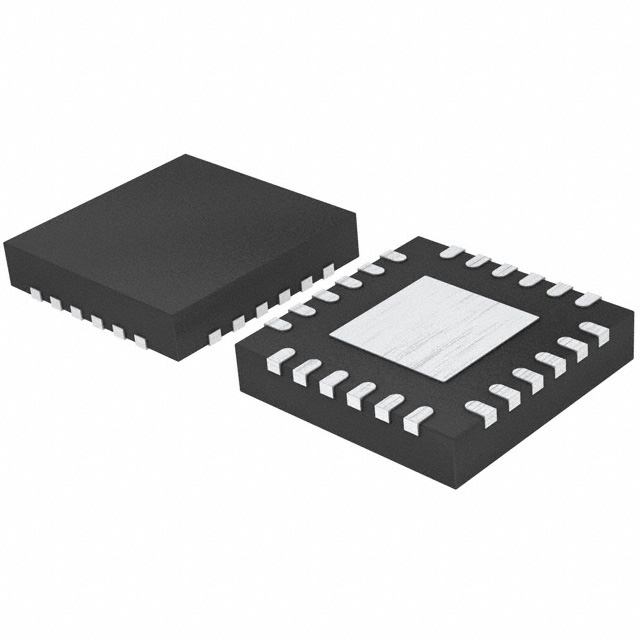
- Package: LFCSP (Lead Frame Chip Scale Package)
- Essence: Analog-to-Digital Converter (ADC)
- Packaging/Quantity: 2500 units per reel
Specifications and Parameters
- Resolution: 12 bits
- Sampling Rate: 100 MSPS (Mega Samples Per Second)
- Input Voltage Range: ±1 V
- Power Supply: +3.3 V
- Operating Temperature Range: -40°C to +85°C
Detailed and Complete Pin Configuration
The ADN2913ACPZ has the following pin configuration:
- VIN-
- VIN+
- GND
- VREF-
- VREF+
- CLK
- DOUT
- GND
- PDWN
- VDD
Functional Characteristics
The ADN2913ACPZ is designed to condition and amplify analog signals for conversion into digital form. It offers high-speed operation, low power consumption, and precise signal processing capabilities. The integrated ADC provides a resolution of 12 bits and a sampling rate of 100 MSPS.
Advantages and Disadvantages
Advantages: - High-speed signal conditioning and amplification - Low power consumption - Precise analog-to-digital conversion - Compact LFCSP package
Disadvantages: - Limited input voltage range - Requires a +3.3 V power supply
Applicable Range of Products
The ADN2913ACPZ is suitable for various applications that require high-speed and accurate analog-to-digital conversion. It can be used in telecommunications, medical imaging, industrial automation, and scientific instrumentation.
Working Principles
The ADN2913ACPZ utilizes advanced analog signal processing techniques to condition and amplify the input signals. The amplified signals are then converted into digital form using the integrated ADC. The resulting digital data can be further processed or transmitted for various applications.
Detailed Application Field Plans
- Telecommunications: The ADN2913ACPZ can be used in high-speed data communication systems to convert analog signals into digital format for transmission and processing.
- Medical Imaging: It can be employed in medical imaging devices, such as ultrasound machines, to digitize the received analog signals for image reconstruction and analysis.
- Industrial Automation: The ADC can be utilized in industrial control systems to convert analog sensor signals into digital data for monitoring and control purposes.
- Scientific Instrumentation: The ADN2913ACPZ is suitable for scientific instruments that require precise analog-to-digital conversion, such as oscilloscopes and spectrum analyzers.
Detailed Alternative Models
- ADN2912ACPZ: Similar specifications and characteristics, but with a lower sampling rate of 50 MSPS.
- ADN2914ACPZ: Similar specifications and characteristics, but with a higher resolution of 14 bits.
5 Common Technical Questions and Answers
Q: What is the maximum input voltage range of the ADN2913ACPZ? A: The maximum input voltage range is ±1 V.
Q: What is the power supply requirement for the ADN2913ACPZ? A: It requires a +3.3 V power supply.
Q: What is the operating temperature range of the ADN2913ACPZ? A: The operating temperature range is -40°C to +85°C.
Q: Can the ADN2913ACPZ be used in low-power applications? A: Yes, it features low power consumption, making it suitable for low-power designs.
Q: What is the package type of the ADN2913ACPZ? A: It is packaged in an LFCSP (Lead Frame Chip Scale Package).
This encyclopedia entry provides an overview of the ADN2913ACPZ, including its basic information, specifications, pin configuration, functional characteristics, advantages and disadvantages, applicable range of products, working principles, detailed application field plans, alternative models, and common technical questions and answers.