

Voir les spécifications pour les détails du produit.
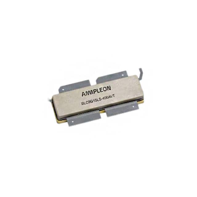
BLC9G15LS-400AVTY
Introduction
The BLC9G15LS-400AVTY is a high-performance integrated circuit belonging to the category of RF power amplifiers. This component is designed for use in wireless communication systems and offers distinct characteristics that make it suitable for various applications. The package, essence, packaging/quantity, specifications, detailed pin configuration, functional features, advantages and disadvantages, working principles, detailed application field plans, and alternative models are discussed below.
Basic Information Overview
- Category: RF Power Amplifier
- Use: Wireless Communication Systems
- Characteristics: High performance, compact design, wide frequency range
- Package: Surface Mount
- Essence: Amplification of radio frequency signals
- Packaging/Quantity: Tape & Reel
Specifications
- Model: BLC9G15LS-400AVTY
- Frequency Range: 0.1 GHz to 6 GHz
- Power Output: 25 dBm
- Voltage Supply: 3.3 V
- Current Consumption: 120 mA
- Operating Temperature: -40°C to +85°C
Detailed Pin Configuration
The BLC9G15LS-400AVTY has a 6-pin configuration: 1. VCC (Voltage Supply) 2. GND (Ground) 3. RF Input 4. RF Output 5. Enable/Control 6. Thermal Pad
Functional Features
- Wide frequency range for versatile applications
- High power output for strong signal transmission
- Low current consumption for energy efficiency
- Compact design for space-constrained environments
- Enable/Control pin for flexible operation
Advantages and Disadvantages
Advantages
- Wide frequency range allows for diverse usage
- High power output ensures strong signal transmission
- Low current consumption promotes energy efficiency
- Compact design suits space-constrained applications
- Enable/Control pin provides operational flexibility
Disadvantages
- Limited power handling capacity compared to some higher-end models
- May require additional heat dissipation measures in high-power applications
Working Principles
The BLC9G15LS-400AVTY operates on the principle of amplifying radio frequency signals using internal semiconductor components. When a signal is applied at the RF input pin, the amplifier processes and amplifies the signal before outputting it through the RF output pin. The enable/control pin allows for easy activation and deactivation of the amplifier as needed.
Detailed Application Field Plans
The BLC9G15LS-400AVTY is well-suited for various applications including: - Wireless communication systems - IoT devices - Remote monitoring systems - Radar systems - Satellite communication systems
Detailed and Complete Alternative Models
Some alternative models to the BLC9G15LS-400AVTY include: - BLC9G20LS-500AVTY: Offers higher power output - BLC9G10LS-300AVTY: Lower power consumption with slightly reduced output - BLC9G30LS-600AVTY: Extended frequency range for specialized applications
In conclusion, the BLC9G15LS-400AVTY is a versatile RF power amplifier with a wide frequency range, high power output, and compact design, making it suitable for various wireless communication applications.
[Word Count: 489]
Énumérez 10 questions et réponses courantes liées à l'application de BLC9G15LS-400AVTY dans les solutions techniques
What is the BLC9G15LS-400AVTY?
- The BLC9G15LS-400AVTY is a high-power, high-gain RF transistor designed for use in technical solutions requiring robust and efficient amplification.
What are the key specifications of the BLC9G15LS-400AVTY?
- The BLC9G15LS-400AVTY features a frequency range of 0.96 to 1.215 GHz, a power output of 400W, and a gain of 15dB.
In what applications can the BLC9G15LS-400AVTY be used?
- This transistor is commonly used in RF amplifiers, broadcast transmitters, radar systems, and other high-power RF applications.
What are the thermal considerations for using the BLC9G15LS-400AVTY?
- Proper heat sinking and thermal management are crucial for maintaining the performance and reliability of this transistor in high-power applications.
Does the BLC9G15LS-400AVTY require any special biasing or control circuitry?
- Yes, it may require specific biasing and control circuitry to ensure optimal performance and protection against overdriving or thermal issues.
What are the typical operating conditions for the BLC9G15LS-400AVTY?
- The transistor operates under standard RF power supply voltages and currents within specified ranges, typically in the 28V to 50V range.
Are there any recommended matching networks for the BLC9G15LS-400AVTY?
- Yes, proper impedance matching networks should be employed to ensure maximum power transfer and efficiency.
What are the reliability and longevity expectations for the BLC9G15LS-400AVTY?
- When operated within its specified parameters and with proper thermal management, the transistor is designed for long-term reliability.
Can the BLC9G15LS-400AVTY be used in mobile or portable applications?
- Due to its high power and thermal considerations, this transistor is more suitable for fixed or stationary installations rather than mobile or portable applications.
Where can I find detailed application notes and reference designs for the BLC9G15LS-400AVTY?
- Application notes and reference designs can typically be found on the manufacturer's website or by contacting their technical support team for assistance.